The varactor is a relatively simple two-terminal solid state device that
utilizes the voltage-variable capacitance of a PN junction. It has provided
new ways of tuning circuits, amplifying signals, generating oscillations,
multiplying and dividing frequencies, automatically controlling frequency,
and performing other tasks in electronics. In many instances the varactor
does its job more efficiently, simply, and economically than other components.
Varactor operation is easily explained in practical terms and may readily be visualized by the reader who has an understanding of semiconductor behavior. To clarify varactor theory, a brief review of fundamental semiconductor and PN-junction theory will be given in this section. In addition, an explanation in practical terms of how capacitance occurs in a junction-and why it varies with voltage-is included.
WHAT IS A VARACTOR?
Every semiconductor diode has some internal capacitance.
Usually, however, this parameter is insignificant; it is intentionally kept as small as practicable so that it will not degrade normal diode operation. (The capacitance of a junction diode is higher than that of a point-contact diode mainly because the junction diode has the larger area.) Basically, a varactor (its name is coined from the term variable reactor) is a special-purpose junction diode.
But it differs from other diodes in one important respect: it has been designed and fabricated expressly to make its junction capacitance useful. Thus, capacitance--which is an unavoidable nuisance in conventional diodes-is deliberately cultivated in the varactor.
It is both novel and useful that this capacitance can be varied at will by varying the voltage applied to the diode.
This phenomenon enables a tiny varactor to do the work of a conventional variable capacitor that is many hundred times larger. Why a diode possesses capacitance and why the latter is voltage variable may be understood by closely examining the nature of the PN junction.
Although all semiconductor diodes and rectifiers (e.g., copper oxide, germanium, selenium, silicon) have inherent capacitance, which limits the highest frequency at which they will operate efficiently, most varactors are made from silicon. The reason for this choice is that this material has excellent temperature characteristics, and diodes made from it have extremely high back resistance. There is one notable exception: Varactors intended primarily for microwave and very low noise applications often are made from gallium arsenide. In external appearance, the varactor resembles a conventional diode or rectifier of the same power class. It may be as small as a 1/10-watt resistor or as large as a power transistor.
Fig. 1-1 shows circuit symbols for the varactor. In this guide we will use the one at A.
VARACTOR SEMICONDUCTOR FUNDAMENTALS
The varactor differs from the conventional diode chiefly in internal features which result from special processing of ...
-----
1. Besides being called by the familiar generic names of varactor, varactor diode, silicon capacitor, and voltage-variable capacitor, this component is also known by various trade names, such as Capsil, Epi cap, Paramp Diode, Semicap, Varicap, and Voltacap.
---------
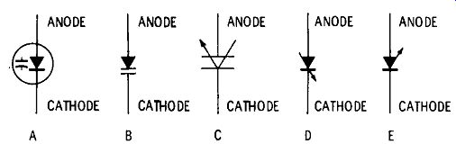
Fig. 1-1. Varactor symbols.
... its semiconductor material and of its junction. This processing ensures usable internal capacitance, high parallel resistance, and low series resistance. The nature and electrical behavior of the semiconductor in the varactor must be examined at the atomic level.
Electricity in Semiconductors
The resistivity of semiconductors suitable for use in varactors lies somewhere between that of good conductors and of good insulators. For example, silicon suitable for this use may have a resistivity of 60,000 ohm-centimeters ( ohm cm) or higher, whereas a good conductor such as copper may show as tiny a value as 1 millionth ohm-cm, and the good insulator mica as high a value as 2 x 10^17 ohm-cm.
The lone vehicle of electric current in common solids, whether conductors or insulators, is the free electron. Metals have enormous quantities of such electrons, insulators barely none. In semiconductors, the electron may not be the sole mobile carrier; current in these materials can be more complicated than in an ordinary conductor or insulator. Be cause a semiconductor can be processed to favor one or an other type of carrier, conditions are obtainable which make diode and varactor operation possible.
Electrons and Holes
Electricity flows through a semiconductor via the drift of two kinds of current carriers: electrons (negative charges) and holes (equivalent positive charges). In semiconductor atoms, the electrons are the particles which orbit around the nucleus ; a hole is a spot at which an expected electron is absent. In a suitably processed material, one type of carrier overwhelmingly predominates, hence is called the majority carrier. The other type is termed the minority carrier and usually exists in inconsequential numbers only. A material is termed N type when its majority carriers are electrons, and P type when they are holes.
Doping
A highly purified semiconductor (which in that refined state is almost an insulator and is termed intrinsic) is deliberately made N type or P type, as desired, by "doping" it with a controlled trace of suitable impurity material (the dopant or additive). In this way, (1) the electrical conductance of the material may be closely tailored, and (2) the type of current carrier may be preselected. Intrinsic silicon, for example, may be made N type by doping it with arsenic or antimony, or P type by doping it with aluminum or boron.
Depending on intended end use, a semiconductor may be lightly doped or heavily doped.
The effect of doping is more complicated than might be guessed from the surface appearance of simply mixing a suitable impurity material into a molten semiconductor. The impurity actually penetrates the semiconductor structure at the atomic level. To understand how this happens, visualize this picture: The atoms in an intrinsic semiconductor are believed to be arranged in an orderly, repetitive pattern called the crystal lattice. The lattice is held tightly together by means of bonds between the electrons of adjacent atoms.
(These so-called valence bonds result from the sharing of orbits by electrons in the adjacent atoms.) Ideally, all of the electrons are tied up in these valence bonds, and at room temperature none are available as current carriers. The atoms of common semiconductors each have four orbiting electrons, each of which forms a bond with an electron in an adjacent atom (see the simplified, two-dimensional representation in Fig. 1-2). Now when an impurity atom is added, it can fasten itself into the semiconductor lattice and be come a part of it only if the impurity electrons form bonds with electrons in the adjacent semiconductor atoms. If an impurity is added which has five valence electrons, each impurity atom will use four of its electrons to bond with adjacent semiconductor atoms, leaving its fifth electron un bonded and free to act as a current carrier. The semiconductor thus becomes N type (see Fig. 1-3). This is what happens when arsenic (five-electron atoms) is added to silicon (four-electron atoms) .
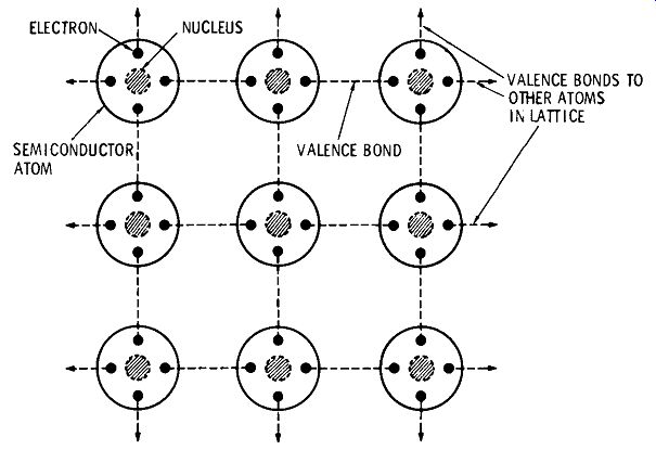
Fig. 1-2. Atoms in intrinsic semiconductor crystal lattice.
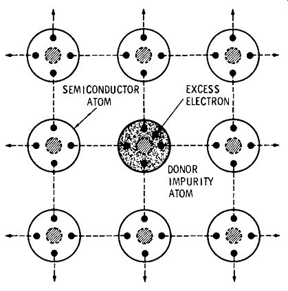
Fig. 1-3. Atoms in N-type semiconductor crystal lattice.
------------
2. If, instead, the dopant is a material whose atoms each have only three valence electrons, each impurity atom will use all three of its electrons to bond with those in adjacent semiconductor atoms. One electron in one of the adjacent semiconductor atoms then has no "mate" in the impurity atom; hence a hole is created in the lattice (see Fig. 1-4). This hole then is free to act as a current carrier ...
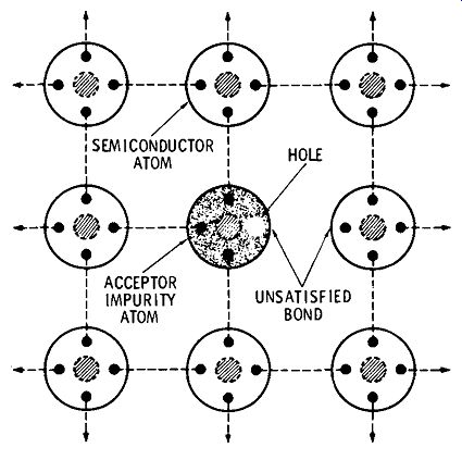
Fig. 1-4. Atoms in P-type
semiconductor crystal lattice.
... (i.e., an available electron from somewhere in the lattice will fall into the impurity-atom hole, leaving a hole where it came from, etc.) and the semiconductor becomes P type.
This is what happens when aluminum or boron is added to silicon. Because the first kind of impurity contributes an electron to the semiconductor, it is called a donor. Similarly, because the second kind of an impurity can take an electron from the semiconductor, it is called an acceptor.
In a typical case, one arsenic atom is added for each 100 million silicon atoms. Very few conduction electrons thus are provided, and this fact accounts for the high resistivity of the doped silicon.
It is well known that the contact between an N-type semi conductor and a P-type semiconductor forms a rectifying "junction." That is, electric current passes through the combination very easily when an applied a-c voltage makes P positive with respect to N, and almost not at all when P is made negative. This shows that the resistance of the junction depends on the polarity of the applied voltage, being low in the first instance and high in the second. This action provides a simple diode-which is basically a PN junction provided with terminals.
Junction Voltage, Current, and Resistance
An applied voltage is termed forward voltage (V_f) when its polarity is such as to make P positive and N negative, and the resulting high current is termed forward current (I_f). Conversely, an applied voltage is termed reverse volt age (V.) when its polarity is such as to make P negative and N positive, and the resulting low current is termed reverse current (I). (Reverse current is also called leakage current.) The corresponding junction resistances are for ward resistance (equal to Vtf J,) and reverse resistance (equal to V./I.) (also called leakage resistance). In PN junctions suitable for varactors, reverse (leakage) current is extremely low-on the order of a few thousandths of a microampere. This is another way of saying that the leakage resistance is extremely high-on the order of several thou sand megohms.
The P layer of the junction is termed the anode, and the N layer the cathode, from the conventional view that current flows through a diode readily when the anode is positive and cathode negative.
Junction Is Internal
Although we conveniently think of the PN junction as the junction between two pieces of semiconductor material, one N and one P, its nature is not so simple. An electrically efficient junction cannot be obtained merely by touching an N type block to a P-type block, however flat their mating faces are polished and however tightly they are pressed together.
The contact must be a great deal more intimate than is af forded by such a simple arrangement. For that reason, the junction is processed into a single block, wafer, or chip of semiconductor material. For example, we can start with a wafer of N-type semiconductor and convert a portion of it to P type. Or, alternatively, we can start with P type and make a portion of it N type. An intimate junction then occurs naturally where the N-type material becomes P type, or vice versa. Finally, a lead may be attached to the N region and another to the P region, for external connection.
Alloyed Junction versus Diffused Junction
Two common methods of making the conversion in a single semiconductor are by alloying and diffusion. In the first, a suitable impurity is alloyed with the semiconductor to convert a part of the semiconductor into the opposite type. During this process, the impurity and the semiconductor both are molten, at least in the region of contact. In the second method, the impurity material is brought into contact with and diffuses into the semiconductor at high temperature but below the melting point (sometimes the dopant is gaseous), somewhat as a drop of ink diffuses into a blotter. Generally, the alloyed junction is abrupt (i.e., the N material quite suddenly becomes P material), whereas the diffused junction usually exhibits gradual transition from N to P. Inside the Junction Diode In a simple PN-junction device (diode, transistor, varactor), why do not the electrons in the N region drift across the junction and fill up the holes in the P region, thereby converting the entire mass into intrinsic semiconductor material and erasing the junction? The answer is that a small amount of this action (termed recombination) does occur when the junction first is formed-a few electrons move into the nearest holes across the junction (Fig. 1-5B). But then, as a result of this initial recombination, that portion of the P region which is at the junction becomes charged slightly negative because of the electrons it has gained, and this charge repels further electrons which try to drift across from the N region. The movement therefore stops. At the same time, that portion of the N region which is at the junction becomes charged slightly positive because of the holes left in it by the electrons it lost in the brief recombination.
This internal electrification is termed the space charge (Fig. 1-5C).
Space-Charge Region
The space charge amounts to a few tenths of a volt and can be imagined as a small battery inside the junction. This voltage (termed contact potential, cp) cannot be measured externally, but we know it is there, because it accounts for several aspects of diode behavior.
(A) N and P materials separate.
(B) N and P materials joined. Re-combination takes place at junction.
(C) N and P materials joined. Recombination completed.
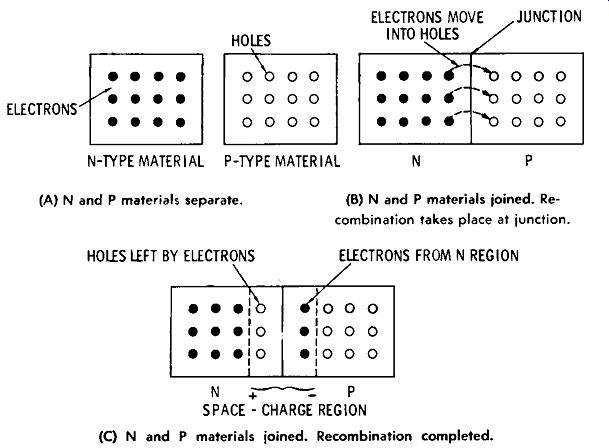
Fig. 1-5. Electron-hole relations at PN junction.
The space charge acts over a narrow section of the semi conductor on each side of the junction-the space-charge region-indicated by the dashed lines in Fig. 1-5C. When no external voltage is applied to the junction, the width of the space-charge region depends on the kind of semiconductor and the degree of its doping. Ideally, no free carriers exist in this region, so it effectively is an insulator, and for this reason is usually called the depletion layer (i.e., depleted of current carriers) .
The behavior of a PN junction in response to applied volt age (bias), briefly previewed earlier under "Junction Volt age, Current, and Resistance," now may be visualized with the aid of Fig. 1-6.
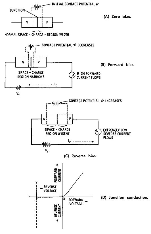
Fig. 1-6. PN junction operation.
Zero Bias
At zero bias, the contact potential (voltage of the .imaginary internal battery) has a characteristic value, and the depletion layer has a characteristic width, as shown in Fig. 1-6A. Both of these are determined by the semiconductor and its processing.
Forward Bias
When the junction is forward biased, as shown in Fig. 1-6B, the external voltage is in series with the contact potential, and electrons from voltage source Vr repel electrons in the N region, forcing them toward the junction. At the same time, the positive electrification from the other pole of source V, repels holes in the P region, forcing them toward the junction. These electrons and holes meet and re combine continuously at the junction, as more electrons enter the N region from the voltage source, and more holes are moved in the P region. The result is the relatively heavy forward current I,. The contact potential is decreased and the width of the space-charge region is narrowed as Vr is increased. When Vr = cp, the space-charge region becomes extremely narrow and eventually disappears.
Reverse Bias
When the junction is reverse biased, as shown in Fig. 1-6C, the external voltage is in series with the contact potential, and the positive charge of the external voltage source, Vr, attracts holes in the P region away from the junction. Here, the result is a widening of the depletion layer, an increase of the contact potential, and a flow of tiny reverse current Ir.
Conduction Characteristic
Fig. 1-6D illustrates the typical forward and reverse currents in a silicon PN junction. From this plot, note that the forward current increases rapidly as the forward voltage is raised. And note that the reverse current is negligible and increases hardly at all as the reverse voltage is raised to a high value, until point X (reverse breakdown voltage Vbr) is reached. At this point the reverse current then increases sharply for a small further increase in reverse voltage. Although this point is termed "breakdown," the junction is not destroyed so long as the reverse breakdown current is limited to a safe value by the circuit in which the junction operates. Conduction, both forward and reverse, is nonlinear over a large part of its range.
Junction Capacitance
The question of how capacitance arises inside the PN junction now may be answered. From the foregoing discussion, it is evident that the junction actually consists of an N (negative) region and a P (positive) region separated by a depletion (intrinsic, insulating) layer. This structure is identical, then, to two flat conducting plates separated by a dielectric. This arrangement describes any two-plate capacitor.
In any two-plate capacitor, the capacitance is directly proportional to the effective area of the plates and to the dielectric constant of the dielectric, and is inversely proportional to the thickness of the dielectric. Expressed as a formula: where, kA C = 4.45d C is the capacitance in picofarads, k is the dielectric constant, A is the area in square inches, d is the thickness of the dielectric in inches.
In the semiconductor junction, A is the area of the N and P regions that face each other across the junction, d the thick ness of the depletion layer, and k the dielectric constant of the depletion-layer semiconductor.
Since the thickness of the depletion layer varies with bias voltage (see Figs. 1-6B and 1-6C), the junction capacitance therefore varies with voltage. In effect, varying the bias voltage "moves" the capacitor "plates" toward or away from each other. That is, the varactor is basically a voltage variable electronic capacitor--the capacitance varying according to the applied voltage.
INSIDE THE VARACTOR
As explained at the beginning of this section, the varactor is a special-purpose junction diode. Specifically, its junction has been processed to optimize capacitance, minimize series resistance, and maximize leakage resistance. Some varactors are fabricated primarily for tuning purposes, others for harmonic generation (frequency multiplication), and still others for parametric amplification and other applications.
Equivalent Circuit
In most applications, the varactor is reverse biased, since in this state it draws virtually no current and, therefore, is essentially voltage operated and consumes almost no power.
The various parameters of the practical varactor are shown in their relation to each other by the equivalent circuit in Fig. 1-7A.
(A) Complete.
(B) Simplified.
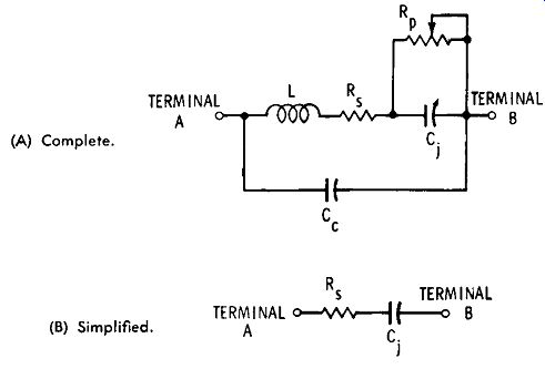
Fig. 1-7. Varactor equivalent circuit.
In Fig. 1-7A, L is the inherent series inductance due to leads and attachments, and to the semiconductor bulk; R. is the series resistance due primarily to bulk resistance of the semiconductor, but also to leads and electrodes; Cc is the stray capacitance of the diode, due to leads, electrodes, attachments, and case; CJ is the internal voltage-variable capacitance of the junction; and RP is the internal leakage resistance of the junction. RP is somewhat voltage variable, since the bias voltage changes the contact potential-see Fig. 1-6.
In practical varactors, L and Cc are reduced as far as practicable through efficient design and packaging. Series resistance R. is minimized and leakage resistance RP maximized through appropriate refinement of the semiconductor and careful control of its doping. Resistance RP often is so high that it may be considered infinite, therefore being of no interest in the equivalent circuit. Junction capacitance CJ is optimized by junction processing and is proportioned by control of junction area, depletion-layer thickness, and semi conductor doping. Because RP is extremely high and L and Ce extremely low, all three may be ignored in many lower frequency situations. The equivalent circuit of the varactor then may be simplified to only two elements: junction capacitance Ci and series resistance R., as shown in Fig. 1-7B. From the foregoing discussion, it is obvious that CJ is the desired parameter and all of the others undesirable but un avoidable. Maximizing Rv renders the varactor essentially voltage operated, by reducing resistive operating current virtually to zero. Minimizing R. increases the Q of the varactor ( here, Q = 1 wR.Ci) , th us reducing internal power losses and sharpening response of the varactor in tuned circuits.3 Minimizing L increases the self-resonant frequency of the varactor.
Capacitance versus Voltage
The capacitance of a varactor varies inversely as the reverse voltage and directly as the forward voltage. The reverse-voltage capacitance is of chief interest in most applications, since at forward voltages leakage current is high and Q low. Therefore, except where specifically designated otherwise, all references to varactor capacitance throughout this guide mean reverse-voltage capacitance.
The capacitance varies nonlinearly. The exact manner in which it varies depends on the type of semiconductor and
--------'One of the methods employed to reduce R, is to dope the semiconductor heavily, but to graduate the doping carefully so that it is light at the actual junction but heavy elsewhere.------------
how it has been processed. For example, in the silicon abrupt-alloyed junction: where, C- K v- y'V+rp Cv is the capacitance at the applied voltage, K is a constant, V is the applied voltage, rp is the contact potential.
The constant (K) depends on the kind of semiconductor and its processing; it is related to reverse breakdown voltage and minimum capacitance of the junction (K is often 1, and rp 0.5 to 0.65 for silicon). In a deep-diffused junction:
K Cv=---
'-3/ V + 'P
Note that only the exponent is different in these two equations-the first denoting the square root of V + rp, and the second the cube root. Through careful management of the diode processing, the exponent can be controlled, in order to tailor the voltage-capacitance curve to individual requirements. Fig. 1-8A shows a typical varactor capacitance curve.
Note that in this instance the capacitance variation is approximately square law. Fig. 1-8B shows the capacitance curve for a particular varactor at both forward and reverse bias.
VARACTOR RATINGS
In their data sheets, varactor manufacturers give mini mum, maximum, and typical values of various operating parameters. These include the following:
1. Maximum Working Voltage (mwv)-The maximum working voltage is the highest reverse voltage ( d-c bias+ peak a-c signal) at which varactor may be safely operated. Depending on type, this is from -9 to -700 vdc.
2. Breakdown Voltage (Vbr)-The breakdown voltage is the voltage at the point at which the reverse current in-creases sharply to a higher level (X in Fig. 1-6D). Some manufacturers specify this voltage for the 10-µ,a point, others for 100µ,a. Depending on type and make, this point will be from -17 to -100
3. Maximum Reverse Current Ur)-The maximum re verse current is the current flow at the maximum re verse working voltage. Depending on type and make, this current ranges from 0.005 to 5 µ,a .
(A) Reverse-voltage capacitance.
CONTACT POTENTIAL
(B) Complete capacitance.
REVERSE VOLTAGE O FORWARD VOLTAGE.
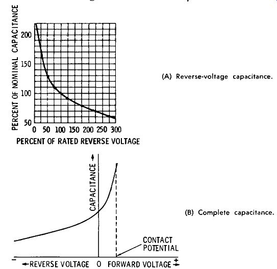
Fig. 1-8. Capacitance versus voltage characteristics.
4. Power Dissipation (Pd)--The power dissipation is the maximum power that can safely be dissipated by the varactor. Depending on type, it ranges from 200 milli watts to 25 watts average at 25°C (up to 450-va reactive power). For operations at ambient temperatures other than 25°C (-263°C to + 200°C, depending on type and make), various manufacturers recommend different de rating factors, usually from 1.67 to 13 mw/°C.
5. Nominal Capacitance (C)-The nominal capacitance is the rated capacitance of the varactor. It is usually stated for a specific voltage (e.g., -4 volts) and frequency ( e.g., 1 MHz). Units are available with values from 0.1 to 2000 pf. The very low capacitances usually distinguish the microwave varactors.
Chart 1-1 lists 48 standard nominal capacitances. These are the figures that appear in the varactor literature or on the varactor case. They are the capacitances obtained at the specified voltage. At lower voltages, the capacitance will be higher, and at higher voltages it will be lower.
Chart 1-1. Nominal Capacitances
All values are in pf.
6. Capacitance Ratio or Range (AC)-The capacitance ratio corresponds to a specified bias voltage range (zero, or a designated level such as -4 volts, to maximum working voltage, -1 to -50 volts, -2 to -100 volts, etc.) and specified test frequency (e.g., 1 MHz). Depending on type, capacitance ratios range from 0.233 :1 to 12 :1.
7. Figure of Merit or Quality Factor (Q)-Q is the ratio of reactance to series resistance ( above 0.1 MHz, Q = 1/w R.CJ and decreases as the frequency increases). It is specified at a particular voltage (e.g., -4 volts) and frequency (e.g., 50 or 100 MHz) and ranges from 3 to 600, depending on capacitance, voltage, type, and make.
At low frequencies (i.e., below 0.1 MHz), Q reaches a value of several thousand. It increases with reverse volt age up to the reverse breakdown point (X in Fig. 1-6D), whereupon it decreases rapidly, approaching zero. Q also decreases rapidly with increasing forward voltage, again approaching zero.
8. Series Resistance (R.)--The series resistance is primarily composed of the bulk resistance of the semiconductor and the resistance of contacts, leads, etc. However, it may also contain in-phase frequency-dependent components, such as constituents of skin effect. It is specified in ohms at a particular bias and extends from 0.14 to 14 ohms, depending on type and make.
9. Cutoff Frequency --The cutoff frequency is the frequency at which Q equals 1. It is generally specified with respect to a particular bias (e.g., -2, -3, -4, or -6 volts, mwv, or l/3Vh.) and extends from 10 to 350 GHz, depending on capacitance, voltage, type, and make.
10. Self-Resonant Frequency--The frequency at which a varactor resonates without external components is the self-resonant frequency. It results from the inherent inductance and capacitance (junction and package capacitances) of the unit. The inherent series inductance is extremely small (typically less than 0.5 nh), so the self resonant frequency accordingly is high. This frequency is not always specified by the manufacturer, but it ranges from 150 to 2000 MHz in lower-frequency models.
11. Forward Current (I_f)-The current resulting from for ward bias of the junction is the forward current. This current is not always specified by the manufacturer, since the reverse characteristics are of prime interest.
However, knowledge of its magnitude is important in some applications where the varactor becomes forward biased during part of a signal cycle, since this condition can, if forward current flows, lower the Q and increase power loss. A typical value for /, is 100 ma at + 1 volt (this is equivalent to a resistance of 10 ohms in parallel with the junction).
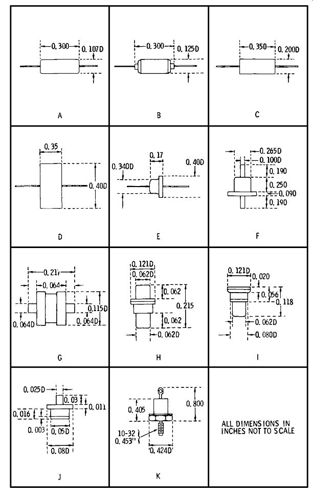
Fig. 1-9. Representative varactor packages.
TYPES OF VARACTORS
Most present-day varactors are made from silicon or gallium arsenide. The diode fabrication is chosen to satisfy various operating requirements. Various configurations are employed: alloyed junction, epitaxial alloyed junction, deep diffused junction, shallow-diffused junction, diffused epitaxial junction, diffused mesa, planar epitaxial, etc. A detailed description of the physical characteristics of these structures or of the manufacturing processes would be extraneous here.
It is sufficient to say that silicon varactors presently are the most widely used, but the more costly gallium-arsenide types find application where the highest Q and cutoff frequency, lowest noise, and highest efficiency at extremely high frequencies are demanded. For example, in microwave frequency multipliers and parametric amplifiers the gallium arsenide type is employed. The epitaxial configuration seems to be most desirable in silicon units.
The packaging of varactors is similar to that of conventional signal diodes and power rectifiers. Fig. 1-9 shows several typical packages, but this is not a complete coverage.
New types are steadily coming forth. Sma L1, hermetically sealed, insulated packages with axial pigtails, as in A, B, C, and D of Fig. 1-9, are no longer than the small resistors or Courtesy TRW Semiconductors
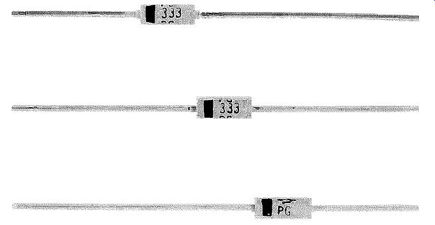
Fig.
1-10. Small-size varactors (TRW PG333).
tubular ceramic capacitors which they resemble (see Fig. 1-10). Various varactors of the type at A and B can handle power up to 500 mw. The one at C can handle 1 watt, and the one at D, 2 watts. A metal-cased, 115-volt unit with axial leads is shown at E. Double-ended ceramic-and-metal cartridges for convenient clipping into vhf and uhf fixtures are depicted at F and G, while H shows a similar double-ended cartridge for microwave use. Parts I and J of Fig. 1-9 show single-ended microwave cartridges of the type often called "pills" because of their shape. Finally, drawing K shows a high-power type. This DO-4 case is identical to that of a power rectifier. The threaded stud permits bolting to a heat sink for cooling. Varactors in this package (K) are rated up to 1 kv or higher, 25 to 30 watts average power, and at frequencies of up to 1200 MHz. Such units are useful in vhf-uhf frequency multiplication and switching.