This section describes some additional applications of varactors, which
are not included in the preceding categories. The ideas are intrinsically
useful and they may also suggest further applications.
There is no intent to suggest that the varactor is a universal component or that it is a panacea. But it is applicable to a number of circuits where it can perform a task more efficiently or simply than devices formerly or presently used for the purpose. Thus, only a few possibilities are explored in this section.
FREQUENCY DIVIDER
Now well known as a frequency multiplier, the varactor will also operate as a frequency divider. It has been used in several ways to achieve subharmonic operation. Fig. 7-1 shows a typical circuit.
In the shunt-varactor circuit of Fig. 7-1, the configuration is essentially the same as that of the frequency multiplier; the chief difference is the tuning of the output filter, L2-C3, to a submultiple (f /n) of the input frequency. Specifically here, the circuit is a frequency halver, i.e., the input is f and the output f /2. Another difference is the noninductive internal load resistor, R2.
The input filter (series-resonant circuit L1-C2) is tuned to the fundamental frequency, f; the output filter (series resonant circuit L2-C3) is tuned to f2. Capacitors C1 and C4 are impedance-matching units for input and output, respectively.
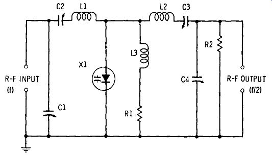
Fig. 7-1. Frequency-divider circuit,
The divider requires a lower self-bias resistance (R1) than is used in multiplier circuits-usually of the order of 1/10 of the multiplier value. In some instances, this (and the presence of R2) precludes efficient operation of the simple circuit shown here alternately as a multiplier or divider simply by interchanging input and output.
Efficiency figures between 80 and 90 percent have been reported for frequency halvers of this type operated with 125-watt input at 50 MHz Uout = 25 MHz). Other configurations (such as parallel-resonant filters, autotransformer input and output, and double tuning) may also be used (see Fig. 4-4.)
MICROWAVE LIMITER
Fig. 7-2 is the block diagram of a relatively simple setup for microwave voltage limiting (compression). A varactor doubler, of any desired configuration, is used with its out-put terminated by a non-radiating, noninductive resistive load, RL, The limiting action afforded by this arrangement is based on an inherent operating characteristic of the varactor doubler: As the applied r-f input is increased from zero, no doubler operation occurs until a characteristic threshold voltage is reached. The doubler then goes into operation, delivering to the load device output power proportional to the input power as the input is further increased. But there is no further increase in r-f input voltage ( which levels off at the threshold value), since the high efficiency of the doubler ...
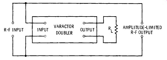
Fig. 7-2. Microwave-limiter circuit.
... causes nearly all of the input power to be converted into output power. The r-f voltage at the output terminals (which are merely extensions of the input pair) therefore is quite constant in amplitude.
This arrangement makes a convenient method for amplitude-limiting microwave and uhf voltages in certain parts of transmitters and signal generators when other schemes prove inadequate.
WAVE FILTERS
The voltage-variable capacitance of the varactor provides an efficient method of tuning several capacitors simultaneously in a constant-K or m-derived filter, using only one control (such as a potentiometer) to do the job. Representative single-section RC filters were shown earlier in Fig. 2-7.
The two types of LC filters for which continuously vari able tuning most often is desirable are the bandpass and bandstop (band-suppression or band-elimination) circuits.
These are shown with varactor tuning in Fig. 7-3. Both are T filters containing appropriate series- and parallel-tuned sections with varactors as the tuning capacitors.
(A) Bandpass.
(B) Bandstop.
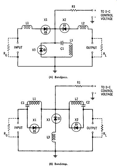
Fig. 7-3. Wave filters.
In the bandpass filter (Fig. 7-3A), the two series arms are the series-resonant elements ( L1- X1 and L2-X2) and the shunt arm is the parallel-resonant element (L3-X3). The DC control voltage is applied to all three varactors simultaneously through the isolating high resistance, R1. The re turn path for this control voltage must be supplied through the output resistance (Ro) of the signal source, for varactor X1; and through the load resistance (Rd, for varactor X2. If these resistances are absent, comparable resistors must be connected in shunt with the input and output terminals. In the shunt arm, DC-blocking capacitor C1 pre vents L3 from short circuiting the control voltage and must be very much higher in capacitance than X3, so as not to tune the shunt arm.
The capacitance ( X1, X2, and X3) and inductance ( L1, L2, and L3) values required for a desired pass frequency and bandwidth may be determined with the aid of standard filter-design formulas or tables.
In the bandstop filter (Fig. 7-3B), the two series arms are the parallel-resonant elements ( L1- X1 and L2-X2) and the shunt arm is the series-resonant element (L3-X3). The DC control voltage is applied to all three varactors simultaneously through the isolating high resistance, R1. The return path for this control voltage must be provided by the output resistance (R0 ) of the signal source, for varactor X1; and by the load resistance (Rd, for varactor X2. If these resistances are absent, comparable resistors must be connected in shunt with the input and output terminals. In the series arms, DC-blocking capacitors C1 and C2 prevent L1 and L2, respectively, from short circuiting the control voltage. The capacitance of C1 and C2 must be very much higher than that of X1 or X2.
The capacitances ( X1, X2, and X3) and inductances ( L1, L2, and L3) required for a desired notch frequency and bandwidth may be determined with the aid of standard filter-design formulas or tables.
VOLTAGE-TUNED Pi NETWORK
The CLC pi network is used in many ways: antenna coupler in transmitters, low-pass wave filter, power supply filter, and phase-shift transmission line are several examples. Both of the capacitors in the network may be DC tuned simultaneously from a single potentiometer if they are varactors as shown in Fig. 7-4.
The transmission and impedance characteristics of the network are determined by the inductance of coil L1 and the capacitances of the two varactors, X1 and X2. The inductance and capacitance values required for a desired mode of operation may be determined with the aid of standard filter-design and phase-shift formulas or tables.
CONTROL VOLTAGE
Fig. 7-4. Voltage-tuned pi filter.
The DC tuning voltage is applied to the two varactors simultaneously--to X1 through r-f filter L2, R1, and C2 and to X2 through r-f filter L3, R2, and C2. R1 and R2 are isolating high resistances. C1 and C3 are DC-blocking capacitors; C1 prevents the input signal source from short circuiting the DC control voltage on varactor X1, and C3 prevents the external load from short circuiting the DC control volt age on varactor X2. Each of these capacitances must be very much higher than the capacitance of X1 and X2, so that the varactors and not the capacitors will determine the network characteristics.
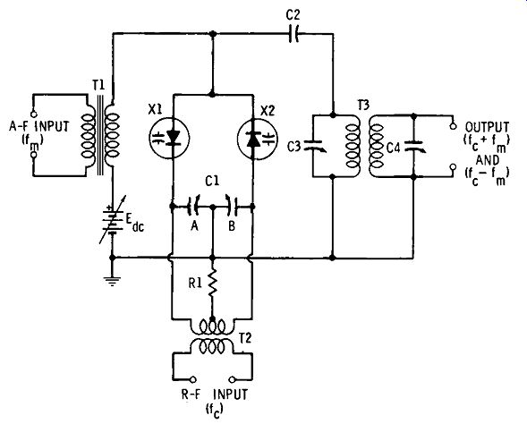
Fig. 7-5. Balanced modulator.
BALANCED MODULATOR
Balanced modulators are used principally in wave analyzers, spectrum analyzers, and sideband transmitters. Fig. 7-5 shows a bridge-type modulator circuit in which two of the bridge arms are varactors ( X1 and X2) and the two other arms are conventional capacitors (C1A and C1B, the two sections of a split-stator variable capacitor). The varactor arrangement is similar to the signal converter shown earlier.
The varactors are biased by adjustable DC voltage Ede to a favorable point for lowest distortion. Direct-current blocking capacitor C2 prevents the primary of transformer T3 from short circuiting the bias . A radio-frequency carrier Ue) is presented to the bridge through air-core trans former T2. If X1 and X2 are capacitance matched and if the sections of the variable capacitor ( C1) track and are equal, this capacitor may be adjusted to balance the bridge, whereupon the carrier will be suppressed at the output terminals. If, then, audio-frequency modulation (/01 ) is applied through transformer T1, the AF voltage will be superimposed on the DC bias voltage, Ede, and will fluctuate the capacitance of the varactors, balancing and unbalancing the bridge at the audio-frequency rate. Each time the bridge is unbalanced, the carrier is switched through transformer T3 to the output terminals (the AF signal cannot pass through this air-core transformer) ; and each time the bridge is balanced, the carrier is cancelled in the output. The output wave therefore contains the sum (f_e + f_m ) and the difference (f_e + f_m) of carrier and audio, but no carrier; i.e., it consists of the upper sideband and lower sideband. Capacitors C3 and C4 permit tuning transformer T3 to the desired side band. Additional selectivity may be provided with a crystal filter resonant at the desired sideband and operated at the output of the circuit.
By careful matching of the varactors and critical adjustment of bias voltage Ede, spurious modulation products may be minimized.
ULTRAHIGH-RESISTANCE SWITCH
Fig. 7-6 shows the circuit of a varactor switch which offers an ultrahigh resistance to a DC switching-signal source.
An r-f signal is switched by a DC voltage. The circuit de livers output as long as the switching signal is maintained, and thus simulates a spst spring-return switch. This application is an adaptation of the basic resonant-slope amplifier.
TO DC CONTROL VOLTAGE AC OUTPUT
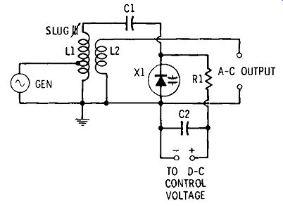
Fig. 7-6. Ultrahigh-resistance switch.
The r-f signal is supplied by the generator and is coupled into coil L1 through an impedance-matching tap. L1 forms a tank with varactor X1, resonant at the generator frequency. Capacitor C1 provides DC blocking, to prevent L1 from short circuiting the DC control voltage. R1 is an isolating high resistance, and C2 an r-f bypass capacitor.
With the DC control (switching) voltage applied to the circuit, the tuning slug of coil L1 is adjusted to resonate the circuit at the generator frequency, as indicated by maximum voltage at the AC output terminals (this voltage is coupled out of the tank by means of L2). When the DC control volt age is removed, the AC output voltage falls to zero, because the tank completely detunes (if the frequency is high enough, e.g., 20 MHz or more). Thus, the output may be switched on and off by making and breaking the DC voltage.
Current drawn from the DC source, which may have as low as 1 volt output, is of the order of nano-amperes; the input resistance of the switch accordingly is of the order of gig ohms. If desired, the switching voltage may be a positive going square wave or pulse. To use a negative switching signal, simply reverse the varactor and the DC input terminals.
The r-f output may be rectified with a single germanium diode (or diode bridge) to give DC output. The DC output obtained in this way will close a sensitive DC relay.
CAPACITIVE POTENTIOMETER
A compact, small-sized AC potentiometer (attenuator, voltage divider) may be obtained with a series connection of capacitor and DC-controlled varactor (see Fig. 7-7). A capacitive potentiometer is called for when power consumption must be held to a minimum and resistive elements are prohibited.
AC OUTPUT
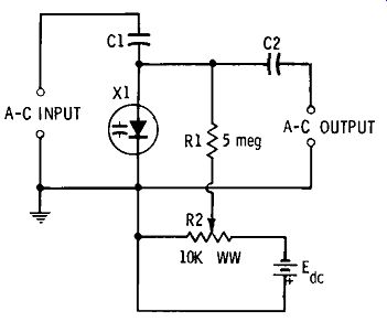
Fig. 7-7. Capacitive potentiometer (attenuator).
The AC input voltage to be controlled is applied across capacitor C1 and varactor X1 in series. The varactor capacitance is varied by means of a DC control voltage obtained through potentiometer R2 from DC source Ede. Resistor R1 serves as isolator and AC choke. The capacitance of C1 must be chosen with respect to the minimum and maxi mum capacitances of varactor X1 so that the desired output voltage range will be obtained as the varactor is "tuned" through its capacitance range.
Capacitor C1 automatically provides DC blocking, to pre vent the input-signal source from short circuiting the varactor DC voltage and to protect the varactor from any direct current present in the input signal, while it acts as the upper arm of the capacitive potentiometer. A separate capacitor, C2, must be provided, however, to protect varactor X1 and its DC voltage from the external load device. The capacitance of C2 must be very much higher than that of the varactor, so that the varactor capacitance, rather than C2, determines the attenuation.
LIGHT-CONTROLLED CAPACITOR
In Fig. 7-8, a varactor receives a variable DC control volt age from a self-generating photocell or solar battery (PC) through the usual isolating high resistance, R1. A high output solar battery will vary the varactor capacitance over a significant range as the cell experiences illumination from total darkness to bright light. Blocking capacitor C1 protects the varactor from any direct current present in the circuit in which this variable capacitor is used, and it pre vents the external circuit from short circuiting the varactor DC control voltage. The capacitance of C1 must be very much higher than that of the varactor, so that the capacitance "seen" at the "capacitance" terminals is principally that of the varactor. Because the varactor draws virtually no current from the ce L1, the cell output voltage will be its maximum no-load value at each level of illumination.
SOLAR BATTERY
CAPACITANCE TERMINALS
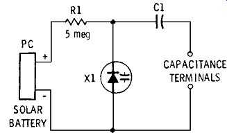
Fig. 7-8. Light-controlled capacitor.
The variable capacitance available at the "capacitance" terminals may be used in a variety of ways. For example, a telemetering transmitter may be tuned by it, to communicate light changes to a distant observer. Or it may be used to shift the frequency of a beat-frequency oscillator in response to the interruption or variation of light. In any application, the amplitude of an AC signal applied to the varactor by the external circuit must be very much less than the photocell DC voltage to prevent overriding the latter.
NEGATIVE REACTOR
(A) Circuit.
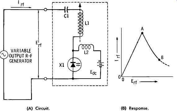
Fig. 7-9. Negative reactor. (B) Response.
Negative reactance (the AC counterpart of negative resistance) has been observed in varactors. This may be seen in a series-resonant circuit comprised by a varactor and conventional inductor and operated with an adjustable AC in put. Such an arrangement is shown in Fig. 7-9A. That part of the circuit within dotted lines may be regarded as the negative reactor. Here, the series-resonant circuit is composed of coil L1 and varactor X1. Capacitor C1 provides DC blocking, and its capacitance must be very much higher than that of X1, so that this capacitor does not tune the resonant circuit.
At a given value of reverse bias ( Ede), the inductance of L1 is set by means of its slug to tune the series-resonant circuit to resonance when the generator voltage, Ert, is one half of maximum. When the generator voltage then is reduced to zero, the circuit current Un) also drops to zero, as shown in Fig. 7-9B. Increasing Ert then causes lrt to in crease, this current reaching a maximum at point A where the signal voltage has tuned the series-resonant circuit to resonance. Increasing Ert further produces a decreasing Irr, since the signal voltage now detunes the circuit above resonance. Current Irr consequently decreases, as from A to B. The negative slope, AB, indicates negative reactance voltage increases; current decreases. This negative reactance is available at the input terminals and may be used in various r-f circuits for monostable switching, generation of lower-frequency oscillations, and similar applications common in negative-resistance practice.
VARACTOR EFFECTS IN CONVENTIONAL DIODES
The sensitivity of capacitance to reverse voltage was first observed in conventional semiconductor diodes. This is a secondary property in such diodes and is minimized to the greatest practicable extent. Nevertheless, it is present in some degree in all such diodes, depending on type and make, and can be exploited when desired.
Junction diodes exhibit the highest capacitance, chiefly because of their larger area, but even point-contact diodes show a small amount. Most manufacturers specify the capacitance in their diode data sheets.
The major practical difference between the conventional diode and the varactor is that of leakage current. The level of this current can be significant in some of the conventional diodes (such as zeners) which give the highest capacitance, e.g., a few microamperes. In spite of this shortcoming, which results in appreciable loading of the DC control voltage source and in internal diode losses, the conventional diode can function as an emergency varactor or as an interesting (and often inexpensive and readily available) unit for demonstrating the DC dependence of junction capacitance.
A diode must be carefully picked from a good sampling if best varactor simulation is desired. Criteria for selection are lowest reverse leakage current throughout the projected range of DC control voltage, and best capacitance for the projected application. (Note that "best" capacitance does not always mean highest capacitance.) The conventional diodes which most nearly meet all of the requirements for varactor substitution are the silicon units. The reverse leak age of germanium diodes totally un-suits them for voltage controlled applications, although they can afford DC control of capacitance if one is willing to expend a certain amount of DC power.