The field-effect transistor (abbreviated FET) is a special semiconductor device. Although it is similar to the regular transistor (technically known as the bipolar transistor), it differs from the latter in several respects. The most important of these is the high input impedance of the FET, compared with the relatively low input impedance of the bipolar transistor. This means that the input signal for a FET can be a voltage at practically zero power level, whereas the input signal of a bipolar transistor must be a current at a significant, though low, power level.
Because the FET employs an input-signal voltage electro statically to control an output-signal current, its operation strongly resembles that of the vacuum tube. The FET shares with the vacuum tube the properties of transconductance and good input/output isolation, in addition to high power gain and voltage-dependent operation. At the same time, because the FET is an active semiconductor device, it also resembles the bipolar transistor. The FET shares with the bipolar transistor the properties of low power-supply requirements, efficient DC power conversion, the control of current carriers in a solid material, small size, light weight, mechanical ruggedness, cool operation, and freedom from microphonics. In several respects, the FET is better than either the tube or the bipolar transistor.
This section describes the FET and explains its operation. The discussion is presented in simple language with a minimum of mathematics, and presupposes that the reader already knows how a conventional bipolar transistor works.
1.1 FET TYPES
The conventional transistor is called bipolar because it employs two types of current carrier (both electrons and holes in a single transistor) in its operation. The field-effect transistor is called unipolar because it employs only one type of carrier ( either electrons or holes, depending on whether the FET is made from N-type or P-type semiconductor material). The field-effect transistor has three principal electrodes: source, drain, and gate. These correspond to the emitter, collector, and base, respectively, of the bipolar transistor, and to the cathode, plate, and grid, respectively, of the vacuum tube. In practical terms, one may think of the drain and the source as the anode and the cathode of the device, and of the gate as the control element. Some FET's are single gate; others are dual gate. Fgr. 1-1 shows a simple black-box representation of a single-gate FET, illustrating the relationship of electrode terminals. A FET is termed symmetrical when the source and drain terminals may be interchanged without affecting its operation. It is termed asymmetrical when the designated source and drain terminals cannot be interchanged without impairing the performance of the device. Most FET's presently manufactured fall into this second class.
Field-effect transistors are classified as junction FET's (JFET's) and metal-oxide semiconductor FET's (MOSFET's). The MOSFET is known also as an insulated gate FET (IGFET) for reasons that will be explained later. Junction FET's may be further classified according to whether the largest portion is made from N-type or P-
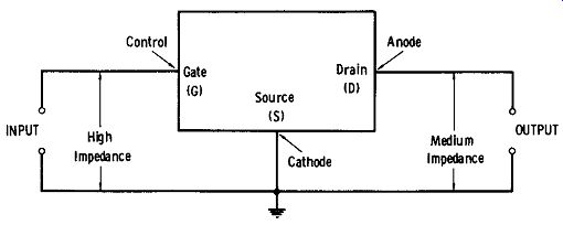
Fgr. 1-1. Black-box representation of a single-gate FET.
type semiconductor material (N-channel JFET's and P channel JFET's, respectively). MOSFET's are classified ac cording to their intended mode of operation ( depletion mode, enhancement mode, or depletion/ enhancement mode, explained later in Section 1.4) and further classified as N channel or P-channel depending on the type of material used for the drain and source. The entire family of field-effect transistors thus may be classified, at this writing, according to the foil owing outline:
I. JUNCTION FET (JFET) A. N-channel JFET (N-type semiconductor)
B. P-channel JFET (P-type semiconductor)
II. METAL-OXIDE SEMICONDUCTOR FET (MOSFET or IGFET) A. N-channel MOSFET
1. Depletion Mode
2. Depletion/Enhancement Mode
3. Enhancement Mode B. P-channel MOSFET
1. Depletion Mode
2. Depletion/Enhancement Mode
3. Enhancement Mode
Additionally, JFET's and MOSFET's may be classified as single gate or dual gate. Most types are the former.
1.2 JFET: STRUCTURE AND OPERATION
Fgr. 1-2 shows the basic structure of the junction field effect transistor (JFET). An N-channel JFET is shown in
Fgr. 1-2A, and a P-channel JFET is shown in Fgr. 1-2B. Some manufactured FET's look quite different from these simple illustrations, but the latter show the basic geometry well enough for purposes of explanation.
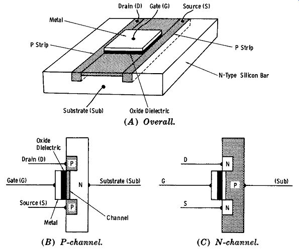
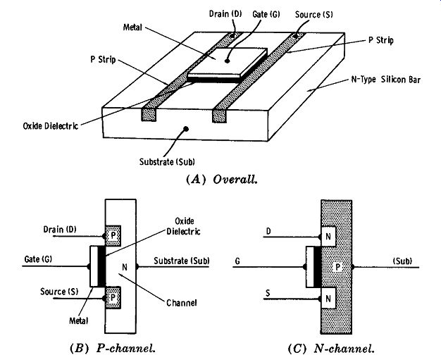
The JFET consists essentially of a small, thin bar of silicon (occasionally germanium) to each end of which an ohmic (non-rectifying) connection (A, B) is made. This silicon bar may be N type (as in Fgr. 1-2A) or P type (as in Fgr. 1-2B). On each opposite face of the bar, a controlled amount of doping material is diffused in to create two, parallel facing strips of the opposite kind of silicon. Thus, two P-type strips are created in the N-type bar (Fgr. 1-2A) where each forms a P-N junction, and two N-type strips
(A) N-channel JFET.
(B) P-channel JFET.

Fgr. 1-2. Basic structure of the junction field-effect transistor (JFET).
are created in the P-type bar (Fgr. 1-2B) where each forms an N-P junction. In a similar fashion, two dots or two squares might be used instead of two strips, provided they are parallel. A connection ( C, D) is made to each of the strips, and the basic FET is complete. One of the end-of-bar terminals (A or B) will be the source electrode, and the other will be the drain electrode. If the FET is symmetrical, either A or B may be the source. The two strip junctions constitute the gate electrode, and are usually tied together internally and connected to a single terminal.
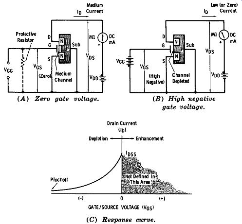
Fgr. 1-3 illustrates JFET operation. In each of the three examples here, an N-channel JFET is shown, and the source electrode is the common (grounded) terminal. The gate-to source circuit is the input, and the drain-to-source circuit is the output. One DC voltage (Vos from the supply Voo) biases the drain/source (output) half, and another DC voltage (Vos from the supply Voo) biases the gate/source (in put) half. In each of the three examples, voltage V ns has the same value.
(A) Zero gate voltage.
(B) Medium gate voltage.
(C) High gate voltage.

Fgr. 1-3. JFET operation.
In Fgr. 1-3A, Vos is zero, and the drain current (In) (S to D in the silicon bar) is relatively high. This current path inside the bar is termed the channel. The drain current in this instance is proportional to the resistance of the channel.
When a moderate voltage, Vos, is applied between the gate and source such that the gate junction is reverse biased, as in Fgr. 1-3B, a depletion layer is set up in the nor mal manner for P-N junctions, around each junction. (A depletion layer is a region that is almost completely free of current carriers; therefore, it acts like a dielectric.) The depletion layers penetrate into the bar, toward each other, and thus reduce the width of the channel. Because fewer current carriers can pass through, In is reduced in value, being proportional to gate voltage Vos- Since the gate junction is reverse biased, there is virtually no gate current; therefore, the gate/source (input) resistance is very high (resistances of 1000 megohms are found in JFET's). When a high reverse voltage (Vos) is applied between gate and source, as in Fgr. 1-3C, the depletion layers penetrate deeper into the bar, further narrowing the channel width and reducing drain current In to a value still lower than that in Fgr. 1-3B. When Vos is sufficiently high, the depletion layers practically touch each other, blocking the channel and reducing In to almost zero. This cutoff point is similar to plate-current cutoff, which occurs in a tube when the negative grid voltage reaches a critical high value.
It is in this way that the JFET uses an input voltage to control an output current. The control mechanism in this operation is the voltage-dependent widening of the depletion layers; and, since the layer is largely the effect of an electrostatic field at the gate junction, the name field-effect transistor applies perfectly. The family of transfer curves in Fgr. 1-4A illustrates JFET operation. From these plots, and the single curve shown in Fgr. 1-4B, note that for a given value of Vos, the drain current increases very rapidly at first as V ns is slowly increased from zero, then reaches a knee and levels off. The corresponding rapid-rise region A from zero to the knee is termed the ohmic region, and I_D in this region is proportional principally to V ns and the channel resistance. The flattened region B is termed the saturation or pinchoff region, and I_D in this region is limited principally by the channel width resulting from the widening of the depletion layers. In region C, which is indicated by the steep, dotted rise of the curve, In increases catastrophically as V ns is increased only a small amount above a critical high value that depends on the model of FET. This latter region is termed the avalanche or breakdown region, and is recognized as similar to the same type of sudden current rise that typifies the performance of zener diodes and avalanche diodes. Unless In is limited (as by means of a suit able external series resistor), operation in region C may result in burnout of the FET. Region A is sometimes called the triode region because the shape of the curve in this region resembles the response of a triode tube. Similarly, region B is sometimes called the pentode region because the shape of the curve in this region resembles that of a pentode tube. The arrangements in Fgr. 1-3, by means of which the performance data shown in Fgr. 1-4 could be obtained, correspond to the common-emitter bipolar-transistor circuit and to the common-cathode vacuum-tube circuit.
(A) Family. (B) Individual.
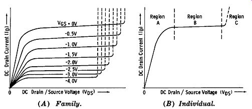
Fgr. 1-4. Typical JFET performance.
In the operation illustrated by Fgrs. 1-3 and 1-4, the gate bias voltage is either zero or negative. It is apparent, how ever, from the curves in Fgr. 1-4A that if the gate/source voltage, V Gs, is made positive, the In values will be higher than those shown in the curves. But if this is done, the gate junction will no longer be reverse biased and, like any other forward-biased junction, it will draw significant current from the V GG supply. The gate-junction resistance accordingly will be lowered, and the high-input-impedance feature of the FET will be lost.
Fgr. 1-3 and the accompanying explanation concern the operation of N-channel JFET's. A P-channel JFET (Fgr. 1-2B) operates in a similar manner. But if a P-channel JFET is used, the polarity of each of the bias supplies (V DD and V GG) and that of the milliammeter (M1 in Fgr. 1-3) must be reversed; i.e., the drain must be biased negative and the gate must be biased positive. Note, however, that the positive gate of the P-channel JFET represents reverse bias, which, in turn, means high gate resistance.
Since the V Gs bias polarity shown in Fgr. 1-3 is correct for high gate resistance, gate current (IG) is virtually zero.
This means that the source current (18 ), corresponding to the cathode current of a tube or the emitter current of a common-emitter-connected bipolar transistor, is in this in stance the drain current, ID. If the gate were forward-biased, as explained two paragraphs ago, then IG would become a significant part of Is.
P-Channel JFET N-Channel JFET P-Channel JFET N-Channel JFET (A) Single gate. (B) Dual gate.
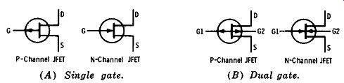
Fgr. 1-5. Circuit symbols for the JFET.
It is interesting to note that in the JFET, current carriers (ID) flow through a single polarity of semiconductor material; they do not flow across junctions as they do in the bipolar transistor. One of the resulting advantages is the absence of the noise components caused by junction currents.
Fgr. 1-5 shows circuit symbols for the junction field-effect transistor. Note that the arrowheads of the gate electrodes point toward the channel in N-channel types and away from the channel in P-channel types.
1.3 JFET/BIPOLAR/TUBE-CIRCUIT COMPARISON
In circuits for performing approximately the same functions, there are many similarities between typical JFET, bipolar transistor, and tube configurations. Fgrs. 1-6 and 1-7 show, for example, comparisons of "common-cathode" and "cathode-follower" type amplifiers, respectively. In each
(A) Common-source N-channel JFET.
( C) Common-source P-channel JFET.
(E) Common-cathode tube.
(B) Common-emitter npn.
Common-emitter pnp.
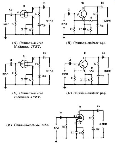
Fgr. 1-6. Comparison: "common-cathode" circuits.
instance, (A) is the N-channel JFET version, (B) the npn bipolar version, (C) the P-channel JFET version, (D) the pnp bipolar version, and (E) the tube version of the circuit.
In each application, the control-electrode DC bias is developed as a voltage drop resulting from the flow of output electrode current carriers through a resistor (R2) connected between the common electrode and ground. This is drain
(A) N-channel JFET source follower.
(C) P-channel JFET source follower.
(B) Npn emitter follower.
(D) Pnp emitter follower.
(E) Tube cathode follower.
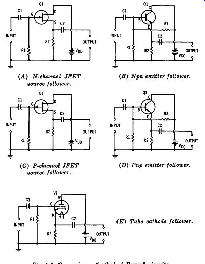
Fgr. 1-7. Comparison: "cathode-follower" circuits.
current in the JFET's, collector current plus base current (therefore emitter current) in the bipolar transistors, and plate current in the tube. In the bipolar circuits (Fgrs. 1-6B and D, and Fgrs. 1-7B and D), additional stabilizing bias is developed by the voltage-divider network R1-R3.
Since bipolar transistors are current-operated devices and the base-bias resistor (R1) is low, their input impedance is low. The JFET and tube, however, are voltage operated devices that have extremely high input resistance.
The grid resistor or gate resistor (R1) therefore largely determines the input impedance of the circuit and may be several megohms, as desired. Because the JFET and tube are high-input-impedance devices, capacitors C1, C2, and C3 in Fgr. 1-6A, C, and E, and capacitors C1 and C2 in Fgr. 1-7A, C, and E may be low-capacitance units (0.1 µF, typical), whereas the same capacitors in the equivalent bipolar circuits (Fgr. 1-6B and D and Fgr. 1-7B and D) must be high capacitance units (1.0 µF electrolytic, typical). Another configuration (not shown in Fgrs. 1-6 and 1-7) that is sometimes employed is the common-gate FET. This arrangement is analogous to the grounded-grid tube amplifier or the common-base bipolar-transistor amplifier.
1.4 MOSFET: STRUCTURE AND OPERATION
A particular feature of the metal-oxide semiconductor field-effect transistor (MOSFET) is its extremely high in put impedance, which is higher than that of either the JFET or the vacuum tube. The reason for this elevated resistance (impedance) will be clear from the following. Two distinct types of MOSFET's exist: depletion and enhancement. They differ in both structure and operation, so they will be discussed separately.
Depletion Type
Fgr. 1-8A shows the basic structure of the depletion-type MOSFET. As was true in the preceding explanation of the JFET, some manufactured MOSFET's look quite different from this simple illustration, but the latter shows the basic geometry of the unit well enough for purposes of explanation. However, the reader is cautioned that these drawings are not to scale; it is impracticable to show the widths and thicknesses of the MOSFET elements in anywhere near the true relationship they have to each other. Thus, although the text calls certain layers thin, those layers must be shown thick in the drawing in order for the reader to see them.
Oxide Dielectric Drain IOI Substrate (Sub)
Drain IOI Gate (GI Source ISi Oxide Dielectric (A) Overall.
D N-Type Silicon Bar Gate(GI Substrate (Sub) G Source ISi Metal Channel (B) P-channel. (C) N-channel.
Fgr. 1-8. Basic structure of the depletion-type MOSFET. (Sub)
Unlike the JFET, the MOSFET does not use a reverse biased P-N junction as a gate. Instead, it uses a thin metal plate, which is insulated from the rest of the structure by an extremely thin dielectric layer. Both the metal plate and the dielectric layer are deposited films. When a voltage is applied to this metallic gate, the resulting electrostatic field penetrates into the semiconductor material of the MOSFET, and is the mechanism whereby the gate voltage may be used to control the current in the semiconductor.
In Fgr. 1-8A, the MOSFET has been made from a bar or plate of N-type silicon. This bar forms a base for the other parts of the device, and is termed the substrate (sometimes called the bulk, base, or body). Two P-type strips (P, P) are diffused a short distance apart into the substrate, and thus form two P-N junctions. One of these junctions acts as the source; the other acts as the drain. A P-type channel is dif fused into the substrate between the two P strips. On the surface of the substrate, over the channel, a thin film of silicon-dioxide dielectric is grown. A thin film of metal is then deposited on top of the dielectric film. The metal-film plate is the gate electrode, and is insulated from the substrate by the dielectric film. It is this characteristic arrangement of metal, oxide, and semiconductor that is signified by the name MOSFET. And it is from the fact that the metallic gate is insulated from the rest of the device that this type of transistor is also known as an insulated-gate field effect transistor (IGFET). While the MOSFET illustrated by Fgr. 1-8A is built on an N-type substrate, the opposite type of structure is also possible; that is, two N regions may be diffused into a P-type substrate. The deposition of the metal and oxide films of the gate is the same as before.
A tiny capacitor is formed by the gate. The metal film is one plate of this capacitor, the facing substrate area is the other plate, and the oxide film is the dielectric. The capacitance is small, usually on the order of 1 to 10 picofarads.
The dielectric film may be only a few microns thick ; as a result, it can be punctured easily (and the MOSFET can be irreparably damaged) by static electric charges that the equivalent capacitor can pick up. For protection of the unit, the manufacturer supplies a MOSFET with its leads short circuited. The protective shorting device must not be re moved until all circuit connections are completed and the MOSFET has been installed. Some MOSFET's have a built in protective zener diode between gate and source, in order to free the user from these precautions in handling.
Fgrs. 1-8B and 1-8C show cross sections of the MOSFET. Fgr. 1-8B features N-type substrate, and Fgr. 1-8C features P-type substrate. In each unit, current carriers will flow from the source, through the channel to the drain. The path between the two P regions in Fgr. 1-8B, or between the two N regions in Fgr. 1-8C, is the channel, and it is the current in this channel that is controlled by the electrostatic field from the insulated gate electrode. Leads are connected to the junctions (for source and drain), to the metal film (for gate), and to the substrate, as shown. In some MOSFET's, the substrate is tied to the source internally.
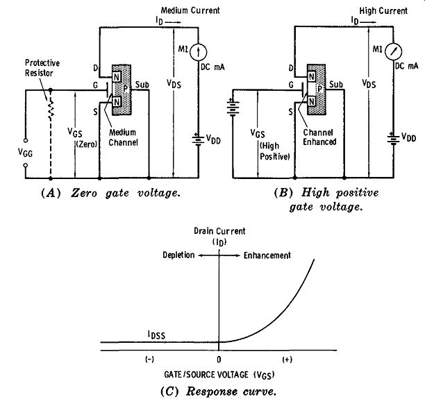
(A) Zero gate voltage. (B) High negative gate voltage. ( C) Response curve.
Fgr. 1-9. Depletion-type MOSFET.
It can be seen from Fgr. 1-9 that the depletion-type MOSFET may be connected for test and measurement in the same manner as the JFET. That is, the source is the cathode and is the common (or grounded) electrode, the drain is the anode, and the gate is the control electrode.
In both of the examples, the drain supply voltage (V DD) has the same value and polarity. Operation of the MOSFET may be explained in the following manner : ( 1) When the gate/ source voltage (V Gs) is zero (Fgr. 1-9A), there is a moderate amount of drain current Io, and this is determined chiefly by the channel resistance and voltage V ns• This action corresponds to the point where the response curve crosses the vertical axis in Fgr. 1-9C. (2) When the gate VOLTAGE is negative (Fgr. 1-9B), the drain current is lower than when V Gs= 0. The reason for this action is the narrowing of the channel due to the negative field from the gate electrode
[the negative charge reduces (depletes) the number of charge carriers in the channel between the drain and source in proportion to V Gs]. This performance corresponds to the curve in Fgr. 1-9C. If the negative V Gs is made high enough, In will be completely cut off ( this corresponds to the pinchoff point in Fgr. 1-9C). (3) When the gate voltage is positive, the drain current is not defined for depletion-type transistors.
While Fgr. 1-9 depicts the operation of an N-channel MOSFET, the same principles apply to the P-channel type, provided the polarities of V GG and V nn and of meter M1 are reversed in each example, and provided the P and N labels are interchanged in the MOSFET symbol.
Enhancement Type
Fgr. 1-10A shows the basic structure of the enhancement type MOSFET. Some manufactured units look quite different from this simple illustration, but 'the latter shows the basic geometry of the unit well enough for purposes of explanation. However, the reader is cautioned that these drawings are not to scale; it is impractical to show the widths and thicknesses of the MOSFET elements in anywhere near the true relationship they have to each other. Thus, although the text calls certain layers thin, those layers must be shown thick in the drawing in order for the reader to see them.
The enhancement-type MOSFET, like the depletion type, uses a thin metal plate which is insulated from the rest of the structure by an extremely thin dielectric layer. Both the metal plate and the dielectric layer are deposited films.
When a voltage is applied to this metallic gate, the resulting electrostatic field penetrates into the semiconductor material of the MOSFET, and is the mechanism whereby the gate voltage may be used to control the current in the semi conductor.
In Fgr. 1-10A, the MOSFET has been made from a bar or plate of N-type silicon. This bar, called the substrate, forms a base for the other parts of the device. The P-type strips (P,P) are diffused a short distance apart into the substrate.
One of these acts as the source ; the other acts as the drain.
(B) P-channel.
(A) Overall.
( C) N-channel.
Fgr. 1-10. Basic structure of the enhancement-type MOSFET. No channel
is diffused into the substrate; this is the distinguishing feature of its
construction. While the MOSFET illustrated by Fgr. 1-10A is built on an
N-type substrate, the opposite type of structure is also possible; that
is, two N regions may be diffused into a P-type substrate. The deposition
of the metal and oxide films of the gate is the same as before.
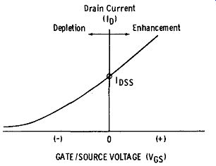
(A) Zero gate voltage. (B) High positive gate voltage.
Drain Current llol Depletion ---t--Enhancement loss (-J GATE/SOURCE VOLTAGE IVGSI ( C) Response curve.
Fgr. 1-11. Enhancement-type MOSFET.
(V Gs) is reversed. Operation of the MOSFET may be explained in the following manner: ( 1) When the gate/ source voltage (V Gs) is zero (Fgr. 1-llA), there is only leakage current between the drain and the source. This action corresponds to the point where the response curve crosses the vertical axis in Fgr. 1-11C. (2) When the gate voltage is positive (Fgr. 1-llB), the drain current is higher than when V Gs = 0. The reason for this action is the enhancement of the channel due to the positive field from the gate electrode (the positive charge produces an N region in the channel between the N drain and N gate, thus providing an N-N-N conduction path). This performance corresponds to the response curve in Fgr. 1-9C. Positive-bias operation is obtained without degrading the high input impedance of the MOSFET. Since the gate electrode is insulated from the substrate by as much as 1 billion megohms, there is no appreciable gate current. This is a definite advantage over both the tube and the bipolar transistor, since the tube will draw grid current, and the corresponding npn bipolar transistor will draw base current when the grid of the tube or base of the transistor is biased positive. The MOSFET has another advantage over the JFET, because driving the junction-type gate of the latter positive in the N-channel JFET, or negative in the P-channel JFET, produces forward current. A MOSFET designed for enhancement-mode operation presents a special case-its channel has extremely high resistance, and therefore is virtually nonexistent until a certain value of positive gate bias is applied. The channel resistance then becomes lower, allowing the conduction of drain current. As the positive gate-bias voltage is increased further, the channel becomes proportionately more conductive (i.e., enhanced).
Fgr. 1-12. Depletion/enhancement MOSFET response curves.
Depletion/Enhancement Type
From the foregoing explanation, one sees two types of construction and operation : ( 1) a negative-bias type operating in the depletion mode, and (2) a positive-bias type operating in the enhancement mode. There is a third type operating between these. The depletion/ enhancement type is so called because when the gate bias is zero, an ac input
Fgrs. 1-10B and 1-l0C show cross sections of the MOSFET. Fgr. 1-l0B features an N-type substrate, and Fgr. 1-10C features a P-type substrate. In each of these units, current carriers can only flow from the source, through the substrate, to the drain. A portion of the substrate between the two P regions in Fgr. 1-10B or between the two N regions in Fgr. 1-10C acts as the channel, and it is the cur rent in this channel that is controlled by the electrostatic field from the insulated gate electrode. Leads are connected to the junctions (for source and drain), to the metal film (for gate), and to the substrate, as shown. In some MOSFET's, the substrate is tied to the source internally.
It can be seen from Fgr. 1-11 that the enhancement-type MOSFET may be connected for test and measurement in the same manner as the JFET and the depletion-type MOSFET. That is, the source is the cathode and is the common (or grounded) electrode, the drain is the anode, and the gate is the control electrode. In both of the examples, the drain supply voltage (V 0o) has the same value and polarity. However, the polarity of the gate-bias voltage signal will drive the gate alternately negative (into the depletion region of the response curve) and positive (into the enhancement region of the response curve). See Fgr. 1-12.
By comparison, JFET operation is ordinarily in the depletion mode only, since operation in the enhancement mode will seriously lower JFET input impedance. Some MOSFET's are designed and manufactured expressly for the depletion mode, some for the enhancement mode, and some for the depletion/ enhancement mode.
Transfer Curves
The transfer curves in Fgr. 1-13 depict the performance of MOSFET's. Note that the slope of the saturation (pinch off) region of the depletion-mode curves (Fgr. 1-13A) is al most horizontal, like those of the JFET (Fgr. 1-4), which also is a depletion-mode device. The slope of the same region of the depletion/enhancement-mode curves (Fgr. 1-13B) varies from almost horizontal at the maximum negative value of V Gs to steep at the maximum positive value of V Gs• The slope of the same region of the enhancement-mode curves (Fgr. 1-13C) varies from almost horizontal at the lowest positive value of V Gs to quite steep at the highest positive value of V GS• The depletion-mode curves resemble comparable pentode-tube curves, whereas the enhancement mode curves resemble comparable bipolar-transistor curves.
Fgr. 1-14 shows circuit symbols for the metal-oxide semi conductor field-effect transistors (MOSFET's). Note that in Fgr. 1-14, drawings (c) and (d), the substrate is connected internally to the source. In all other instances, an external connection to the substrate is provided.
(A) Depletion mode.
(B) Depletion/enhancement mode.
( C) Enhancement mode.
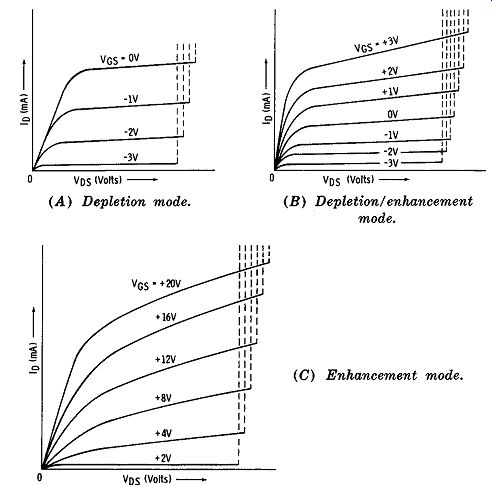
Fgr. 1-13. Typical MOSFET performance curves.
(A) Single gate. (B) Dual gate.
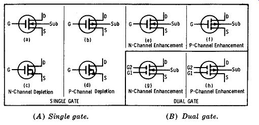
Fgr. 1-14. Circuit symbols for the MOSFET.
1.5 MOSFET IN TYPICAL CIRCUITS
Fgr. 1-15 shows three versions of the common-source MOSFET amplifier circuit, which is comparable to the common-cathode tube, common-emitter bipolar transistor, and common-source FET circuits (see Fgr. 1-6 for comparison). In Fgr. 1-15A, automatic negative DC gate-bias voltage
(A) Negative gate bias ( depletion mode) . ( C) Positive gate bias ( enhancement mode) .
(B) Zero gate bias (depletion/enhancement mode) .
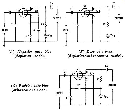
Fgr. 1-15. MOSFET common-source circuits.
is obtained from the voltage drop across R2 produced by the source current. The MOSFET here consequently operates at negative Vos; i.e., in the depletion mode. In Fgr. 1-15B, the source is grounded directly and the DC gate-bias voltage is zero. The input ac signal therefore can swing the gate positive on one half-cycle and negative on the other; the MOSFET here accordingly operates in the depletion/ enhancement mode. In Fgr. 1-15C, positive DC gate-bias volt-age is obtained from the drain power supply (V DD) through the R1-R2 voltage divider. The MOSFET here accordingly operates in the enhancement mode. Each MOSFET is constructed to operate in one of these three modes. The reader who is familiar with tube and transistor circuits will recognize that there are other ways of obtaining negative and positive gate-bias voltage. For example, a fixed gate-voltage source (V GG) might be used. The circuits shown in Fgrs. 1-15A, B, and C, however, offer single-battery simplicity.
Fgr. 1-16 shows a simple source-follower circuit, which is comparable to the cathode-follower tube, emitter-follower bipolar transistor, and source-follower JFET circuits (see Fgr. 1-7 for comparison).
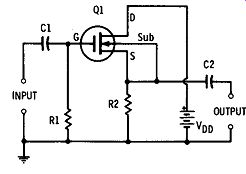
Fgr. 1-16. MOSFET source-follower circuit.
Another configuration (not shown in Fgrs. 1-15 and 1-16)
that may be used is the common-gate MOSFET. This arrangement is analogous to the grounded-grid tube amplifier and the common-base bipolar transistor amplifier.
In all of the circuits in Fgrs. 1-15 and 1-16, N-channel MOSFET's are shown. P-channel units may also be employed, provided the battery (V DD) is reversed in each in stance. It should also be clear how other single-gate MOSFET's from the group shown in Fgr. 1-14 might be employed in these circuits.
The MOSFET in all of its applications exhibits the special feature of extremely high input impedance, and this property reduces practically to zero any loading that the MOSFET imposes upon a driving source. In the circuits in Fgrs. 1-15 and 1-16, therefore, the input impedance is determined principally by the resistance of gate resistor R1, which may be several megohms, as required.
1.6 FET RATINGS
Obviously, a large number of electrical characteristics may be used to specify a FET and describe its operation, since different models (like different tubes and bipolar transistors) often have unique properties. It is impracticable and far from mandatory in this introductory treatment to list all of these here. The list that follows is thought to explain the core of ratings applying to most FET's.
Because the FET, like the tube, is basically an electrostatic-control device, it makes possible the use of a small input voltage to control a large output current (hence, amplification). From this, it follows that the most important FET characteristic perhaps is transconductance, as trans conductance expresses the extent to which this control is achieved. Transconductance (gr.) is equal to the change in drain current (dlD) divided by the change in gate voltage ( dV 0 ) and the formula is often written as follows:
gr.= 1000 (dln/dVo)
where, gt• is the transconductance in micromhos, ID is the drain current in DC mA, Vo is the gate/source voltage in DC volts.
These and other characteristics follow. All of these figures depend on the FET make and model.
Common-Source Forward Transconductance (gr.)
The ratio of din to dV os•
Similar to tube transconductance (Gm). Given for a specified VDs, Vos, and f = 1 kHz. Range: 35 to 50,000 µ,mho.
Common-Source Output Conductance, Input Shorted (go •• )
Reciprocal of drain/source output resistance. Given for specified V Ds, Vos, and f = 1 kHz. Range : 1 to 600 µ,mho.
Common-Source Input Capacitance, Output Shorted (C1 ) Capacitance between gate and source. Given for specified V Ds, Vos, and f = 1 kHz. Range: 2 to 65 pF.
Common-Source Reverse Transfer Capacitance (Crss)
Given for specified V Ds, V Gs, and f = 1 kHz. Range: 0.02 to 6 pF. Drain Current at Zero Gate Voltage (IDss)
The current in the drain/source circuit (i.e., through the channel) when V Gs = 0. Given for specified V Ds•
Ranges:
0.1 to 10 mA at V Ds = 5 V, 5 to 25 mA at V Ds = 8 V, 0.03 to 6.0 mA at VDs = 10 V, 0.2 to 20 mA at VDs = 15 V, 0.4 to 7.5 mA at VDs = 20 V, 80 to 250 mA at VDs = 35 V. Drain Cutoff Current (ID OFF)
Leakage current through the channel when V Gs has been adjusted for cutoff of output. Given for specified VDs and VGs• Range (for VDs = 15 V): 0.05 nA at VGs = 5 V, to 0.07 nA at V Gs= 10 V. Gate/ Drain Voltage (V GD) Also called drain/gate voltage. The maximum voltage that may appear between the gate and drain electrodes.
Range: 20 to 50 Vat 25°C. Gate Reverse Current (IGss)
Also called gate leakage current. The reverse current in the gate/source circuit. Given for VDs = 0 and a specified value of V Gs• Range: 2 nA at V Gs= 15 V, 10 pA to 0.5 nA at VGs = 20 V, 0.1 to 30 nA at VGs = 30 V. Gate/Source Breakdown Voltage (BV Gss)
The voltage at which the gate junction of a JFET will enter avalanche. Given for IG = 1 µ,A and V Ds = 0. Range: 20 to 50 V at 25°C. Gate/Source Pinchoff Voltage (Vr)
The gate-to-source voltage at which the field just closes the conduction channel. Given for ID= 1 nA, 10 nA, or 1µ,A, and for a specified value of Vns ( e.g., 5 to 15 V).
Range:
0.6 to 50 V.
Gate/Source Voltage (V Gs)
Also called source/gate voltage. The maximum voltage that may appear between the gate and source electrodes.
Range: 20 V to 50 V at 25°C. Noise Figure (NF) Internal noise generated by the FET. Given for V Gs= 0, and at a specified Vos (e.g., 15 V) and frequency (e.g., 1 kHz, 200-Hz bandwidth). Range: 0.5 to 3 dB for JFET's.
Somewhat higher in MOSFET's.
Total Device Dissipation (P) Maximum power that can be safely dissipated by the FET structure. Range: 200 mW to 0.8 Win free air at 25°C. Common-Source Parallel Input Resistance (rGs)
The resistance between the gate and source electrodes.
Given for a specified value of drain/source voltage and drain current (e.g., Vos=10 V, lo=0.15 mA). Typical values: 10^9 ohms for JFET's, 10^15 ohms for MOSFET's.
1.7 FET PACKAGING AND APPLICATION
Like bipolar transistors, FET's are commercially avail able in a variety of packages ranging from plastic encapsulation to small metal cans. Various basing schemes are employed, so the manufacturer's literature must be consulted for identification of terminals. In some models, one of the electrodes (usually the gate) is tied internally to the metal can, and these FET's must be installed with care to prevent shorts, grounds, or stray pickup. In some models, a separate pigtail is tied to the can.
The family of field-effect devices has now grown to impressive size. Depending on the FET model, field-effect circuits can be employed at frequencies from DC to several hundred megahertz (the Type 40673 MOSFET, for example, is rated to 400 MHz). This wide operating range allows the FET to be used in all types of communications, instrumentation, and control equipment. The designer selects a FET to suit his purpose much as he would choose a tube or bipolar transistor. Matched pairs of FET's are available for balanced circuit operation, and matched N-channel and P-channel units are available for complementary symmetry operation.
At this writing, the FET is essentially a small-signal device; its power output is limited to the milliwatt region.
However, integrated circuits are appearing in which FET's are used in the input circuit to provide high input impedance, and the power output of some of these integrated circuits can be expected to be usefully higher than that of a FET alone.