One way to get acquainted with the field-effect transistor is to experiment with it on a breadboard. In this way, using a minimum of parts and the few common test instruments found on any electronic hobbyist's equipment shelf, the experimenter can observe firsthand how the FET works. He can also check performance against the FET manufacturer's data.
This section describes, step-by-step, a number of simple tests for the breadboard checking of FET's. The procedures apply in general to any field-effect transistor, provided care is taken to hold voltages, currents, resistor values, and instrument ranges within the limits dictated by a particular type. Where a particular type FET is shown, it is the type that was used in the author's test setup, and the accompanying test data is given for that individual transistor. How ever, other comparable types will operate in the circuit and will yield similar data.
Before the reader who has had no experience with FET's undertakes any of the tests, we recommend a careful study of Section 2.1. This will reduce the chance of damaging the FET's or obtaining misleading data.
2.1 HINTS AND PRECAUTIONS
All of the correct procedures for handling bipolar transistors, with which we assume the reader is already familiar, are also valid for the FET. Nevertheless, some of these are repeated below or paraded in new dress simply because they need re-emphasis here. Certain precautions, however, apply especially to the FET; the MOSFET in particular requires special handling. The reader should study all of the hints and precautions listed below, since the FET is more easily damaged than is the bipolar transistor, and is more susceptible to improper operation.
DC Supplies
All DC supplies must be clean; i.e., their output must contain the minimum of ripple or noise. Ripple voltage and noise voltage can cause all sorts of mischief in test circuits.
The ripple or noise component of a DC voltage used to bias a FET gate, for example, looks like an ac input signal (which, indeed, it is) and gets amplified unintentionally to reappear as a much bigger signal in the FET output. New batteries make the best DC supplies for experimental testing. But many transistor experimenters will want to use ac-operated supplies that they already own. This is permissible if the ripple or noise voltage is accounted for in the interpretation of test results, or if extra filters are used with the supply.
Electrode Voltages and Currents
Hold all electrode DC voltages and currents within manufacturers' ratings. That is, do not exceed the maximum specified DC or peak-to-peak values for drain/source VOLTAGE, gate/source voltage, gate/substrate voltage, drain/gate voltage, drain/substrate voltage, and drain current.
It is always good practice to have voltages smoothly adjustable so that they can be set to the exact desired value.
This calls for continuously variable supplies. When batteries are used, a simple potentiometer (the wirewound volume-control type is permissible) may be connected across the battery to provide an adjustable voltage as shown in the "bias-box" unit in Fgr. 2-1. A limiting resistor ( R1) is connected in series with the battery (B1) and potentiometer (R2) to hold the output voltage to a safe maximum. (For example, if B1 = 22.5 V and the output voltage to be applied to a specific FET must never exceed 12 V, the ratio of R1 to R2 must be chosen such that the maximum output of the potentiometer is 12 volts.) For a given maximum potentiometer resistance (R2), required maximum output voltage (E2), and available battery voltage (E1), the required value of the limiting resistor ( R1) may be calculated:
R1 = [ (El/E2) - l]R2 (2-1)
Thus, if a 10,000-ohm potentiometer and 22.5-V battery are available, and a maximum safe output voltage of 12 V is required,
R1 = [(22.5/12) -1]10,000 = (1.875 -1)10,000 = (0.875) 10,000 = 8750 ohms.
If a fixed resistor having the exact calculated value of R1 is not available, a rheostat can be used in its place. The rheostat can be preset to the required resistance with the aid of an ohmmeter or output voltmeter.
In the schematics in this section, variable batteries are shown for simplicity, but the DC bias voltages may be sup plied, as explained earlier, either by ac-operated supplies or by bias-box supplies.
AC Signal Voltages
Ac signal voltages should be kept as low as practicable. The lowest value that will afford a reliable test should always be used. A good rule of thumb is to restrict the peak value of the signal voltage to 1/10 or less of the DC bias voltage at the FET electrode to which the signal is applied. In any event, respect the maximum values specified by the FET manufacturer. When a FET is operated close to the non linear portion of its response curve, the signal voltage often must be reduced even lower than the 1/10 figure would re quire, to prevent driving into the distortion region.
For the simple tests described in this section, ac signal voltages may be supplied by oscillators or signal generators.
Service-type instruments will be entirely adequate. For high-precision measurements, laboratory-type instruments are required. An audio test oscillator should have low harmonic distortion, but this is no problem, since even service type instruments in this category show well under 1 percent total distortion.
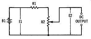
Fgr. 2-1: "bias-box" unit
Current and Voltage Meters
The milliampere and microampere ranges of a service type multimeter are satisfactory for DC current measurements. Only in the measurement of drain cutoff current (see Section 2.4) is an extremely sensitive meter, a pico-ammeter, required. But because such tiny currents do not even deflect the lowest-range service-type microammeter, most practical experimenters will safely call these currents zero. Some vacuum-tube voltmeters and equivalent transistorized voltmeters with current ranges are not recommended here because their insertion resistance is too high.
The insertion resistance should be as low as possible, in or der to create the least upset of a circuit into which the meter is connected. Whereas the insertion resistance of a non electronic multimeter, such as the Simpson Model 260, on its milliampere ranges may be on the order of 25 ohms, that of a VTVM adapted for current may be 1000 ohms or higher.
The sensitivity of the ac voltage ranges of most non electronic multimeters runs around 1000 to 5000 ohms per volt, and this is too low in some instances to prevent over loading of high-impedance circuits. Also, the frequency response of such ac meters sometimes falls off rapidly within and beyond the top of the audio spectrum. For low-level ac signal-voltage measurements, therefore, an ac vacuum-tube voltmeter/millivoltmeter is recommended. (Many technicians own such a meter, since it has long been available in kit form.) This type of voltmeter usually has a constant input resistance of 10 megohms on all ranges. The ac ranges of a regular VTVM or transistorized voltmeter may be used if full-scale deflections lower than 1.5 volts are of no interest. However, the user should be aware that the input resistance of such instruments is lower on the ac ranges than the traditional 11 megohms of the DC ranges. Some oscilloscopes are sensitive enough for ac millivolt measurements, but some of these instruments have an input resistance of only 1 megohm.
Oscilloscope
An oscilloscope is invaluable for showing waveform simultaneously with amplitude of a signal. Thus, signal Voltages (and currents) may be measured, distortion estimated, noise level observed, and signal clipping noted. However, as in the case of the regular VTVM on its ac ranges, the input impedance of a service-type oscilloscope is sometimes low enough that its loading effect must be considered.
Special Instrumentation
The sophisticated experimenter who wishes to look critically into FET performance may require other instruments not shown in the simple test procedures in this section.
Such instruments include a harmonic distortion meter, inter modulation meter, capacitance meter, temperature-test sys tem, noise meter, frequency meter, and phase meter.
General Handling and Testing of FET's
While transistors, like other solid-state components, are relatively rugged mechanically and electrically, they can be damaged through mishandling and careless test procedures. The following is a list of some do's and don't's in this regard.
( 1) A void needlessly dropping a FET or otherwise subjecting it to severe mechanical shock.
(2) Do not operate a FET near hot components. If a test requires operating the FET at high tempera-ture, derate according to the manufacturer's instructions.
(3) Avoid exceeding maximum current and voltage levels even temporarily.
( 4) Follow standard transistor procedure when installing a FET. Use a socket or good clip leads. If you solder the FET into a circuit, grip each lead as you solder it, with long-nose pliers, and continue to hold the lead until the soldered joint and lead have completely cooled.
(5) Install the FET last in the circuit. Complete all other wiring beforehand. A safe sequence is to complete the circuit wiring; check the wiring; attach the DC supplies, signal source, and output device, but with all DC and signal voltages switched off; carefully install the FET; switch-on the DC supplies; and switch-on the signal source. When disassembling a test setup, the following procedure is safe: Switch-off the signal voltages; switch-off the DC voltages; disconnect the signal source; disconnect the DC supplies; and remove the FET.
(6) A MOSFET requires special handling. Do not re move its protective short-circuiting device until all the MOSFET leads have been connected. If you solder the MOSFET into the circuit, observe the pre cautions given in (4) and (5); and, in addition, ground your soldering iron to a good earth connection, such as a cold water pipe. It is a good idea also to ground yourself. Even when grounded, a soldering gun is tricky to use since it may induce a voltage kick in the MOSFET; it is better to use a pencil-type soldering iron.
(7) Never allow the gate of a MOSFET to float. It can easily pick up a static charge that will puncture its dielectric film and permanently damage the MOSFET. Connect a resistor between gate and ground ( even as much as several megohms, if necessary, to simulate an open circuit).
(8) All FET's, unlike bipolar transistors, have a high input impedance, and this makes them susceptible (as vacuum tubes are) to stray pickup. This means that you must keep any possible signal-emitting component away from the FET. You must also keep your body away from an operating FET-FET's are quite sensitive to body capacitance. To prevent body capacitance disturbances when making VOLTAGE measurements, use a shielded probe, and even then keep your fingers well back of the probe tip.
Keep all FET-circuit input-signal leads as short as practicable.
(9) When a MOSFET has an external substrate terminal, connect this terminal to the source terminal, unless otherwise instructed.
(10) Remember that the electrical characteristics of FET's spread over a significant range (note that the manufacturer's data sheet gives minimum, maximum, and typical values), and this variation can cause test results to differ from those given by an author or designer. If you desire to mass pro duce a circuit, or to offer it for duplication, use typical FET characteristics in your design, and even then make your guarantees well inside the performance limits you observe in your tests of the circuit.
(11) Observe the correct polarity of each electrode VOLTAGE.
2.2 CHECKING DRAIN CHARACTERISTIC
The test setup shown in Fgr. 2-2 permits the experimenter to observe how DC drain current (Io) varies with DC drain/ source voltage (Vos) for various values of gate/source DC voltage (V Gs). The procedure is to hold V Gs at a constant value while Vos is varied over an appreciable range, and to note corresponding values of Io.
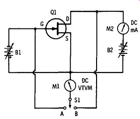
Fgr. 2-2. General-purpose test setup.
A dc VTVM or transistorized voltmeter (M1) is used to measure both V Gs and V ns, and must have an internal polarity shifting switch; otherwise, its input leads must be interchanged when moving from the negative gate to positive drain, and vice versa. A single-pole double-throw changeover switch (S1) allows this meter to read gate/ source voltage in position A and drain/source voltage in position B. The DC milliammeter (M2) must read accurately the range of I_D values to be expected from the FET manufacturer's data; usually, 0-10 and 0-20 mA ranges will suffice. Similarly, the output of the variable DC supplies (B1 and B2) must cover the range of V 0 8 and V ns values, respectively, indicated by the FET manufacturer's data.
(1) Set polarity of meter M1 to negative.
(2) Throw switch S1 to A.
(3) Set B1 to desired gate/source voltage, starting at zero. The value is indicated by Ml.
(4) Throw S1 to B.
(5) Set polarity of meter M1 to positive.
( 6) Set B2 to zero, indicated by M1. Record.
(7) Read corresponding drain current, indicated by M2.
(8) Set B2 to next higher drain/source voltage. Record.
(9) Read corresponding drain current. Record.
(10) Similarly, increase drain/source voltage in small steps, noting drain current at each step. The results when plotted give a single curve similar to Fgr. 1-4B, Section 1. This curve corresponds to zero gate/source voltage.
( 11) After a complete set of measurements has been made (Steps 1 to 10), change the gate/source VOLTAGE to the first desired negative value and repeat the whole series of steps, to obtain a second V ns/ln curve. Then, set the gate/source voltage to a second, higher negative value and repeat the steps.
Repeat this procedure at a full set of gate/source voltage values. The final result will be a family of curves similar to Fgr. 1-4A, Section 1. If operation at positive gate/source voltage also is to be ob served, reverse B1 and repeat the measurements of In vs Vos,
The test circuit and DC polarities in Fgr. 2-2 are given for an N-channel JFET. For a P-channel JFET, reverse B1, B2, M1, and M2. If a MOSFET is under test, the polarities shown here are correct for an N-channel MOSFET in the depletion mode, and the corresponding curves are shown in Fgr. 1-13A. For a P-channel MOSFET in the depletion mode, reverse the polarity of B1, B2, M1, and M2. For a MOSFET in the enhancement mode, the gate/source VOLTAGE must be positive for N-channel and negative for P channel units, and the corresponding curves are shown in Fgr. 1-13C. For a MOSFET in the depletion/enhancement mode, the gate/source voltage must include both positive and negative values, and the corresponding curves are shown in Fgr. 1-13B.
2.3 CHECKING GATE/SOURCE PINCHOFF VOLTAGE
Use the same test setup shown in Fgr. 2-2, except substitute a low-range DC microammeter ( one capable of reading 1 µA) for milliammeter M2. This test shows the gate/source voltage value required to cut off the drain current. Actually, the drain current is never completely cut off, but reaches an extremely low value. A value (such as 1 µ,A) is specified by the FET manufacturer, together with the test value of drain/source voltage (e.g., 10 V). (1) With meter Ml, set B1 to zero and B2 to 10 V (or to any other value of drain/ source voltage specified by the FET manufacturer). (2) Set S1 to A.
(3) Increase voltage of B1, noting that drain current, indicated by meter M2, decreases. Stop when M2 reads 1 µA. (4) At this point, read the corresponding gate/source voltage from meter Ml. This is the desired gate/ source pinchoff voltage.
The test circuit and DC polarities in Fgr. 2-2 are given for an N-channel JFET. For a P-channel JFET, reverse B1, B2, M1, and M2. If a depletion-type or depletion/enhancement type MOSFET is under test, the polarities shown here are correct for an N-channel MOSFET; for a P-channel MOSFET, reverse the polarity of B1, B2, Ml, and M2. For enhancement-type MOSFET's, the polarity of B1 will need to be reversed.
2.4 CHECKING DRAIN CUTOFF CURRENT
The characteristic checked here is the extremely low value of drain current at a specified value of drain/source voltage when the gate/source voltage has been set at a relatively high value. It can be measured only with a very sensitive current instrument (substituted for milliammeter M2 in Fgr. 2-2), since it is usually in pico-amperes (pA). The test conditions are specified by the FET manufacturer ( e.g., V DS = 5 V, V GS = 10 V). Use the test setup shown in Fgr. 2-2, except replace milli ammeter M2 with a DC pico-ammeter.
(1) With meter M1, set B2 (i.e., VDs) to 5 V and B1 (i.e., Vas) to 10 V ( or to any other value of drain/ source voltage and gate/source voltage specified by the FET manufacturer). (2) Read corresponding drain cutoff current from meter M2.
The test circuit and DC polarities in Fgr. 2-2 are correct for N-channel JFET's and MOSFET's. For P-channel JFET's and MOSFET's, reverse B1, B2, Ml, and M2. If an enhancement-type MOSFET is under test, reverse the polarity of B1.
2.5 CHECKING DRAIN CURRENT AT ZERO GATE VOLTAGE
The drain current of interest here is that static value present when the drain/source voltage is a value (such as 10 V) specified by the FET manufacturer, and the gate/ source voltage is zero.
Fgr. 2-3 shows the test setup. In this arrangement, resistor R1 ( 1 megohm or higher) prevents the gate from floating. This resistor may be omitted in some JFET tests, but it is mandatory, to prevent damage, in MOSFET tests.
(1) Set B1 for 10 V (or to any other value of drain/ source voltage specified by the FET manufacturer), as indicated by meter M1.
(2) Read the corresponding drain current from meter M2.
The test circuit and DC polarities in Fgr. 2-3 are correct for N-channel JFET's and MOSFET's. For P-channel JFET's and MOSFET's, reverse B1, M1, and M2.
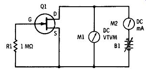
Fgr. 2-3. Setup for checking drain current.
2.6 CHECKING TRANSCONDUCTANCE
Unless the experimenter has access to a dynamometer type ac milliammeter, transformer-coupled ac milliammeter, or transconductance meter (all of which are expensive and uncommon even in some engineering laboratories), he will be unable to measure FET transconductance under ac conditions. A reasonably adequate experimental test may be made, however, with a DC circuit in which the gate/source voltage is varied in two small steps about a mean value, to simulate the peak states of an ac test signal. The corresponding drain current shift is noted, and from the voltage and current values, the forward transconductance (gr.) is calculated.
The test setup shown in Fgr. 2-2 is used.
( 1) With meter M1, set B1 and B2 so that the operating point of the FET is in the center of the flat portion (saturation region) of the response curve. The curves plotted in Section 2-2 may be used to locate this point.
(2) With S1 thrown to position A, record the corresponding gate/source voltage as V1 and the corresponding drain current (from meter M2) as I1• From here on in the test, the voltage of B1 will be varied, but that of B2 will be held constant.
(3) Leave switch S1 in position A.
( 4) Increase B1 for a voltage 0.5 V higher than V 1• Record as V2. (Note that the drain current decreases.)
(5) Read the new current value from M2. Record as 12 .
(6) Decrease B1 for a voltage 0.5 V lower than V1• Record as Va. (Note that the drain current increases.)
(7) Read the new current value from M2. Record as Ia.
(8) Calculate the transconductance:
(2-2)
where, gr. is in u-mho, I2 and Ia are in mA, V 2 and Va are in volts.
The battery and meter polarities shown in Fgr. 2-2 are correct for an N-channel JFET and a depletion-type MOSFET. For a P-channel JFET or MOSFET, reverse B1, B2, M1, and M2. For a zero-biased MOSFET ( depletion/ enhancement mode), V1 will be zero, V2 = +0.5 V, and Va= -0.5 V.
2.7 STATIC TEST OF TRANSCONDUCTANCE
The procedure outlined in the preceding section is a simulated dynamic test that approximates the ac measurement of transconductance. A simpler static test setup is shown in Fgr. 2-4. While the dynamic test is preferable for demonstrating the control properties of the FET, the simpler test is useful in emergencies and requires a minimum of equipment. In this test, the FET gate/source voltage initially is zero. It is then shifted by a known amount (say, 1.5 V). The corresponding drain-current change is noted, and the transconductance is calculated from the voltage and cur rent increments.
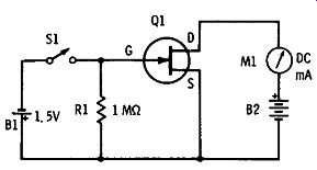
Fgr. 2-4. Setup for static test ~ of transconductance.
The voltage of battery B2 may be any value that will operate the FET within the saturation region of its drain voltage/drain current curve, usually between 6 and 10 volts.
DC milliammeter M1 should have a 0-10 or 0-20 mA range.
The voltage of battery B1 must be known with reasonable accuracy.
(1) Record the voltage of battery B1 as V. (2) With switch S1 (which may be a single-pole single throw normally open pushbutton) open, note the reading of meter M1. Record as l1, (3) Close switch S1, noting that the drain current, indicated by M1, decreases. Record this new reading as l2, ( 4) Calculate the transconductance: where, gt. is in µ,mho, I1 and I2 are in mA, V is in volts.
If B1= 1.5 V, this simplifies to: gt. = 1000 (I1 - I2) /1.5 which further simplifies to: gt.= 667 (11 - 12)
(2-3)
(2-4)
(2-5)
The arrangement in Fgr. 2-4 shows an N-channel JFET; however, the battery and meter polarities are correct also for an N-channel depletion- or depletion/enhancement-type MOSFET. For a P-channel JFET or a P-channel depletion type MOSFET, reverse B1, B2, and M1.
2.8 CHECKING VOLTAGE GAIN
The performance of the FET in a simple amplifier circuit will interest the newcomer to FET circuits. Fgr. 2-5 shows a single-stage, common-source audio amplifier with audio ..
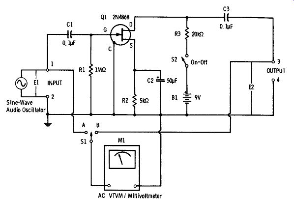
Fgr. 2-5. Setup for checking voltage gain.
... oscillator and ac vacuum-tube voltmeter/millivoltmeter connected for gain measurements. The 2N4868 JFET shown here is metal encased, and a separate terminal (C) is pro vided for grounding the case.
(1) Open switch S2.
(2) Throw switch S1 to position A.
(3) Set output control in oscillator to zero.
( 4) Set oscillator frequency to 1000 Hz.
(5) Set M1 to its 100-mV range.
(6) Close switch S2.
(7) Slowly increase oscillator output until M1 reads 20 mV. Record this value as E1.
(8) Switch M1 to its 1-V range.
(9) Throw switch S1 to position B.
(10) Observe new reading of M1. Record this value as E2.
(11) Calculate the open-circuit voltage gain:
(2-6)
where, E1 and E2 are both in V or mV. The 2N4868 in this experimental setup drew a drain cur rent of 0.3 mA and provided a voltage gain of 20 at 1000 Hz.
However, individual FET's of the same type may show more or less gain, depending on their position in the manufacturer's tolerance spread. The input-signal amplitude (Ed could be increased to 50 mV rms, to give a corresponding output-signal amplitude (E2) of 1 V rms before peak clipping of the output signal was observed with an oscilloscope connected to output terminals 3 and 4.
The experimenter should vary R2 and R3, noting the corresponding voltage gain and also the maximum input signal voltage that may be applied before output-peak clip ping.
A similar circuit may be set up for checking other types of FET's. Battery polarity is correct in Fgr. 2-5 for the N channel JFET shown, and also for N-channel depletion-type MOSFET's. For P-channel JFET's and depletion-type MOSFET's, reverse battery B1. For FET's other than the 2N4868, resistances R2 and R3 must be calculated or worked out by cut-and-try methods. The gate of the enhancement type MOSFET cannot be biased by the source resistor (R2) method at all, but must receive positive bias from a voltage divider (see Fgr. 1-15C, Section 1). A zero-bias (depletion/ enhancement-type) MOSFET would have its source grounded (see Fgr. 1-15B, Section 1), and the ac input signal would drive the gate alternately positive and negative.
If the reader desires, and has the necessary test gear, he can check the simple amplifier ( Fgr. 2-5) in the conventional manner for frequency response, harmonic distortion, output impedance, phase shift, and noise level.
2.10 CHECKING OSCILLATOR ACTION
The readiness of the FET to oscillate may be checked with any simple oscillator . circuit. Fgr. 2-6 shows an untuned crystal oscillator (FET version of the Pierce circuit) that can be used for this purpose. Any quartz crystal (XTAL in Fgr. 2-6) will do; remember, however, that a harmonic-type crystal oscillates in this circuit at its fundamental frequency, not at the labeled frequency, which is a harmonic.
The 2N3823 FET shown here is a metal-encased unit, and has a separate terminal ( C) for grounding the case. In the author's test setup, drain current was 1.8 mA for a B1 VOLTAGE of 6 V.
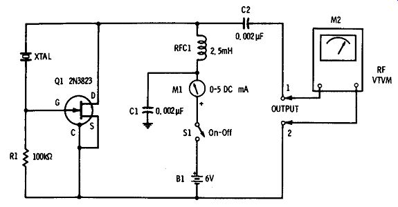
Fgr. 2-6. Setup for checking oscillator action.
1. Set up circuit, as shown in Fgr. 2-6.
2. Connect rf voltmeter (vacuum-tube or equivalent transistorized version) to output terminals 1 and 2.
3. Close switch S1, noting deflection of DC milliammeter M1 and rf voltmeter M2. The author's circuit delivered rf output of 5 V peak to the voltmeter, with a 7000 kHz crystal.
4. The output signal may be transmitted to a receiver or rf frequency meter for monitoring or frequency checking, by means of an antenna connected to output terminal 1. This antenna can consist of 1 or 2 feet of stiff wire or rod vertically mounted, or a few feet of insulated, flexible wire strung either horizontally or vertically. Keep all antennas as short as possible, how ever, since the oscillator makes a fair transmitter capable of radio interference.
2.11 FET CONDITION CHECKING
When a user wants to find by a single test whether a FET is good or bad, he may check transconductance. And when time is important, he may prefer the simple test given in Section 2.7 to the more time-consuming one in Section 2.6, especially if he has a number of FET's to check. But there are also specific test instruments for the purpose, and the service technician certainly will own one of them. These include transistor testers and combined tube/transistor testers.
Not all transistor testers, and tube testers that also test transistors, are satisfactory for testing FET's. Some of these carry the caution "not for FET's or MOSFET's." A few modern transistor testers and combined tube/transistor testers will test FET's in and out of circuit. Most of these latter instruments give a dynamic test of transconductance, employing an internally generated ac signal (e.g., 5 kHz). At this writing, at least one service-type tester is designed for FET's only, and affords both in-circuit and out-of-circuit tests for all types, including dual-gate MOSFET's.
One way of getting acquainted with FET's is to observe the transconductance of several types, using a transistor tester. In this way, the newcomer may note the basic amplifying ability of the FET and contrast it to the transconductance of tubes and the beta of bipolar transistors. Only one simple, relatively inexpensive instrument is required.