This section displays a number of typical applications of the FET in all types of circuits. These examples show the wide range of the uses of the device, but by no means exhaust the possibilities. While the circuits given here are primarily for illustration, the experimenter will be able to set up a selected one for operation with his own FET by means of design and performance equations given in section 3 and the additional data given here. The confirmed experimenter will undoubtedly prefer the breadboard approach for determining optimum operating values for circuit components.
For a collection of practical, predesigned circuits, see the author's book FET Circuits, published by Howard W. Sams & Co., Inc.
4.1 BASIC AF AMPLIFIERS
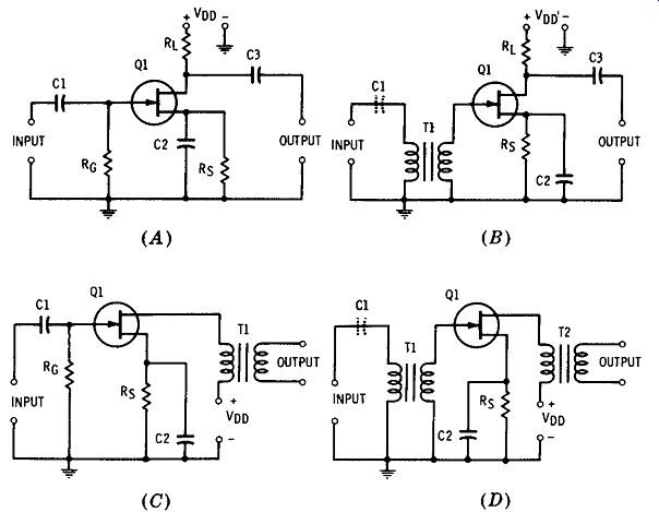
Fgr. 4-1 shows basic single-stage FET audio-frequency amplifiers in various combinations of RC and transformer coupling. Fgrs. 4-1A to D show common-source circuits; Fgrs. 4-1E to H show source-follower circuits. An N-channel JFET is shown in each circuit, but another type of FET may be used, provided the polarity of V DD is reversed where required. For working out the DC bias values for the circuits, see Equations (3-1) to (3-4), in Section 3. The single stage circuits may be cascaded in any combination to secure a desired overall amplification.
Fgr. 4-1A shows a common-source amplifier with RC in put and RC output. This is perhaps the most common arrangement in audio-frequency systems, since it is both simple and compact, and is often the least susceptible to interference. Equations (3-5) to (3-7), in Section 3, depict DC sign and performance of this circuit. If bypass capacitor C2 is omitted, the voltage gain will decrease, but fidelity will be improved as a result of negative feedback developed across resistor Rs [see Equations (3-8) to (3-10), in Chapter 3].

Fgr. 4-1. Basic audio-amplifier circuits.
Because of the high input impedance of this circuit, such stages are easily cascaded, with no signal-voltage loss between stages. Correctly, each succeeding stage should be gate-biased higher than the preceding one, to accommodate the higher signal-voltage level that it receives; this is standard multistage amplifier design. But, for simplicity, identical stages often are cascaded, and the input-signal voltage to the entire system is reduced.
Fgr. 4-1B shows an amplifier with transformer input (T1) and RC output. This arrangement enables a certain amount of voltage step-up to be obtained through the transformer, rather than with an additional amplifier stage. The high input impedance of the FET imposes virtually no load on the transformer. When the transformer primary winding must be protected from a DC component in the input signal, blocking capacitor ( C 1) may be inserted.
Fgr. 4-1C shows RC input and transformer output. This arrangement allows either a signal-voltage step-up or step down, as required, to be obtained at the output of the amplifier. When this type of stage is followed by an RC-input stage, such as in Fgr. 4-1A, T1 becomes an interstage coupling transformer-and the second stage, because of its high input impedance, imposes virtually no load on the transformer.
In Fgr. 4-1D, both input and output are transformer coupled (T1, T2). Any required combination of signal-voltage step-up or step-down may be obtained by proper selection of transformer turns ratio. If the T1 primary winding must be protected from a DC component in the input signal, a blocking capacitor (C1) may be inserted.
Fgr. 4-1E shows a conventional source follower with RC input and RC output. Equations (3-11) to (3-13), in Chap ter 3, depict design and performance of this circuit. This arrangement is often used to provide high input impedance for a lower-impedance device. Thus, a source follower may be followed in cascade by a common-emitter bipolar-transistor RC-coupled stage. In this way, the high input impedance of the FET and the high-voltage amplification of the bipolar transistor are available, and the bipolar circuit thus becomes compatible with such high-impedance devices as the crystal microphone, piezoelectric transducer, etc.
Fgr. 4-1F shows a source follower with transformer input (T1). Here also, Equations (3-11) to (3-13), in Chap ter 3, depict design and performance. The input transformer allows any desired step-up or step-down of input-signal VOLTAGE. The high input impedance of the FET reduces virtually to zero any loading of the transformer. If the primary winding of T1 must be protected from a DC component in the input-signal voltage, a blocking capacitor (C1) may be inserted.
Fgr. 4-1G shows a conventional bootstrap circuit. This arrangement is convenient when a source follower is needed with input impedance higher than that ordinarily obtained with a JFET, and low input capacitance. Equations (3-14) to (3-16), in Section 3, depict design and performance.
This circuit, with its added advantages, is usable for the same functions as those afforded by the conventional source follower ( Fgrs. 4-1E and F). Fgr. 41H shows a bootstrap circuit with transformer input (T1). Here, as in Fgr. 4-1G, Equations (3-14) to (3-16), in Section 3, depict design and performance. Blocking capacitor C2 is necessary to prevent the secondary winding of T1 from short-circuiting the R0 -Rsi-Rs2 bias network. If the primary winding of T1 must be protected from a DC component in the input-signal voltage, another blocking capacitor (C1) may be inserted as shown by the dotted symbol.
As in the other circuits with transformer input, T1 allows any desired step-up or step-down of signal voltage simply by appropriate selection of its turns ratio.
4.2 BASIC RF AND I-F AMPLIFIERS
Fgr. 4-2 shows basic single-stage FET radio-frequency and intermediate-frequency amplifiers. MOSFET's are shown in two of these circuits ( Fgrs. 4-2A and 4-2D), and JFET's are shown in the other two ( Fgrs. 4-2B and 4-2C). However, any desired type of FET may be used in any of these circuits, provided the V DD polarity and the circuit constants-particularly the drain resistor and V DD magnitude are correctly chosen for that type (see Section 3). For Class-A operation, the bias levels for a given FET will be the same as for the basic af amplifiers described in Section 4.1. When, instead, high harmonic content is desired (as when the amplifier is used as a frequency doubler, tripler, or quadrupler), the biases and rf input-signal voltage are adjusted for operation near the ohmic ("triode") region of the FET characteristic. Source bypass capacitors (C3 in Fgr. 4-2A, C2 in 4-2B, and C2 in 4-2D) and drain-supply by pass capacitors (C7 in Fgr. 4-2A, C3 in 4-2B, C3 in 4-2C, and C3 in 4-2D) must be chosen for lowest practical reactance at the signal frequency.
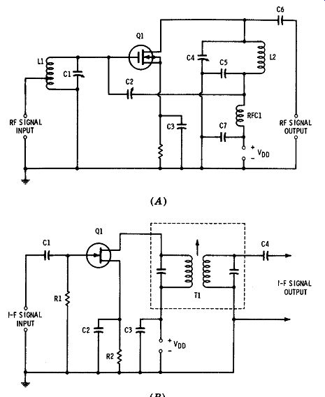
Fgr. 4-2. Basic rf and i-f amplifier circuits.
Fgr. 4-1A shows a conventional tuned-input/tuned-output rf amplifier. This is a well-known circuit in tube and transistor practice (receivers, transmitters, and instruments), and may be used at any frequency at which FET Q1 is capable of operating, including intermediate and audio frequencies. The input tank (L1-C1) and output tank (L2-C4) both are tuned to the desired signal frequency.
Since this condition encourages oscillation, a neutralizing capacitor (C2) has been provided (sometimes, it is desirable to supply the DC drain voltage at a tap on inductor L2 and to connect C2 to the bottom of that inductor). The input signal is presented to the input tank through a suitable impedance-matching tap on inductor L1; however, this signal may also be inductively coupled into L1 by means of a suit able coupling coil, or capacitively coupled into L1 through a capacitor connected to the top of Ll. Similarly, capacitive output coupling is provided by capacitor C6; this results in high output impedance. Output coupling may also be obtained through a low-impedance tap on inductor L2 or through a suitable output-coupling coil. In receiver service, C1 and C4 are ganged.
Fgr. 4-2B shows an i-f amplifier with untuned input and tuned output (i-f transformer T1). An advantage of this arrangement is that, lacking a resonant input circuit, the amplifier is not so likely to oscillate as is its double-tuned counterpart. The input circuit is high impedance; therefore, this amplifier may readily be connected to a signal source, such as a receiver front end, without introducing signal loss.
When an input i-f transformer is used (as in Fgr. 4-2D), the circuit may or may not tend to oscillate, depending on stage gain and the drain/gate capacitance of the FET. If it does oscillate, however, the circuit may easily be neutralized (see Fgr. 4-2A). Fgr. 4-2C shows a common-gate rf amplifier. This arrangement is comparable to the grounded-grid vacuum-tube amplifier and common-base bipolar-transistor amplifier.
Particular advantages of the common-gate circuit are its ability to operate without neutralization up to ultrahigh frequencies, and the presence in its output of both the input rf driving power and the Q1 rf output power. This circuit is particularly useful in FET transmitter circuits; e.g., the Type 2N3823 JFET, which gives a power gain of 10 dB at 200 MHz in this circuit, with a DC power input of 0.3 W, and the Type U222 JFET, which is capable of 0.8 W dc power input.
Fgr. 4-2D shows a dual-gate MOSFET i-f amplifier circuit with provision for automatic gain control. This circuit has been used, as shown, without neutralization; however, it may easily be neutralized (see C2 in Fgr. 4-2A) should it oscillate as a result of input/output tuning (i-f transformers T1 and T2). The age level is set by a positive voltage developed at one gate of the MOSFET by the DC drain-supply voltage divider, R1-R3. A reverse age bias is also applied to the same gate through isolating resistor R2.
4.3 BASIC OSCILLATORS
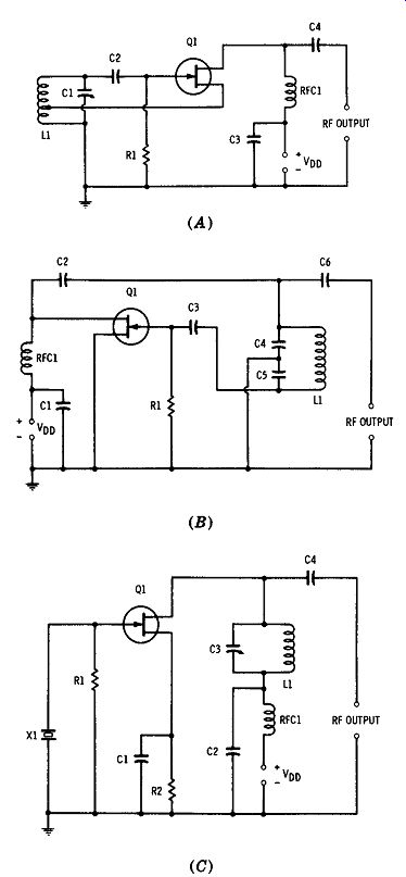
Fgr. 4-3 shows basic single-stage FET rf and af oscillators. Although JFET's are shown, FET's of other types also may be used, provided the V DD polarity and circuit constants--particularly the source resistor and V DD magnitude--are correctly chosen for that type (see Section 3). For sine-wave output, Class-A bias levels must be used, and will be the same as for the basic af amplifiers described in Section 4.1. When, instead, high harmonic output is desired (as when the rf oscillators are used as frequency standards or as drivers for doubler, tripler, or quadrupler stages), the DC gate voltage may be adjusted to a point that will ensure signal-voltage overdriving of the gate. In all of the circuits, source bypass capacitors (C1 in 4-3C, C1 in 4-3D, C3 in 4-3E, and C4 in 4-3F) and drain-supply bypass capacitors (C3 in Fgr. 4-3A, C1 in 4-3B, C2 in 4-3C, C2 in 4-3D, C1 in 4-3E, and C6 in 4-3F) must be chosen for the lowest practical reactance at the signal frequency.
Fgr. 4-3A shows a Hartley-type rf oscillator. In this well known circuit, tapped inductor L1 serves as an autotransformer in which output-signal current in the lower section of the winding induces a gate/source feedback voltage across the upper section.(The frequency of oscillation (f) equals 1/6.28__/L1c1, where f is in hertz, L1 is in henrys and C1 is in farads.) For sine-wave output, the tap must be placed at 1/3 to ½ the distance from the grounded end of L1, the exact point affording the best compromise between signal-output voltage and sinusoidal waveform. The capacitance output coupling (through C4) shown here provides high output impedance, and may be used only with light loading, and even then only when the load will not detune or stop the oscillator. Inductive output coupling (low or high impedance, as desired) may be obtained by means of a suitable output coil coupled to the lower end of L1.
Fgr. 4-3B shows a Colpitts-type rf oscillator. This circuit is distinguished by the split-capacitor (C4-C5) tuning, and is often used in instruments such as dip oscillators. A particular advantage of the Colpitts circuit is its allowance of an untapped inductor. In this circuit, DC gate-bias voltage is developed by the rectified gate/source current through resistor R1. With some FET's, especially MOSFET's, this method may not work, and a source resistor/capacitor combination (such as C1 and R2 in Fgr. 4-3C) must be inserted between source and ground to obtain the required bias. The capacitance output coupling (through C6) shown here pro vides high output impedance, and may be used only with light loading, and even then only when the load will not DC tune or stop the oscillator. Inductive output coupling (low or high impedance, as desired) may be obtained by means of a suitable coil coupled to the center of L1.
Fgr. 4-3. Basic oscillator circuits.
Fgr. 4-3C shows a conventional, tuned-drain crystal rf oscillator. This circuit is comparable to the tuned-plate vacuum-tube or tuned-collector bipolar-transistor crystal oscillator. For oscillation, the output tank (L1-C3) simply is tuned to the crystal frequency. The capacitive output coupling (through C4) shown here provides high output impedance, and is satisfactory only for light loading, and even then only when the load will not detune or stop the oscillator. Inductive output coupling (low or high impedance, as desired) may be obtained by means of a suitable output coil coupled to the lower end of LL
Fgr. 4-3D shows a conventional Pierce crystal oscillator.
This circuit requires no tuning: simply plug in the crystal (Xl), and obtain rf output. However, it oscillates at the fundamental frequency of a harmonic-type crystal, not at the labeled (harmonic) frequency. The Pierce circuit makes a very simple frequency spotter if its gate bias is adjusted for a rich harmonic rf output. In this way, a 100-kHz crystal will furnish check points every 100 kHz apart, far into the radio spectrum (see also Fgr. 2-6, in Section 2). The capacitive output coupling (through C3) shown here pro vides high output impedance, and is satisfactory only for light loading, and even then only when the load will not DC tune or stop the oscillator. Lower-impedance output, when required, may be obtained by capacitance coupling the rf output from the top of resistor R2 after omitting bypass capacitor C1. With some FET's, however, omission of the bypass capacitor will reduce the gain of the circuit to such an extent that oscillation will cease (see Section 3.3, in Section 3). Fgr. 4-3E shows a transformer-feedback af oscillator. In this circuit, signal voltage is fed from the output (drain) section back to the input (gate) section by transformer T1, which is poled correctly for regeneration. Here, the secondary winding (L2) of the transformer is tuned by capacitor C2 (f )=( 1/6.28__/L2C2), where f is in hertz, L2 is in henrys, and C2 is in farads). But either winding may be tuned if it has sufficient inductance. The turns ratio of the transformer must be such that the FET gate is not over driven by the fed-back signal. This, together with Class-A DC gate bias, is essential for sine-wave output. The capacitive output coupling (through C4) shown here provides high output impedance, and is satisfactory only for light loading, and even then only when the load will not detune or stop the oscillator.
Inductive coupling (low or high impedance, as desired) may be obtained by means of a third (output) winding on transformer T1. Lower-impedance output may be obtained by capacitance coupling the af output from the top of resistor R1 after omitting bypass capacitor C3. With some FET's, however, omission of the bypass capacitor reduces the gain so greatly through degeneration that oscillation ceases (see Section 3.3, in Section 3). For output isolation, this oscillator may be followed by a source-follower stage ( Fgrs. 4-1E and G). Fgr. 4-3F shows a phase-shift-type af oscillator. In this circuit, tuning is entirely by means of resistances and capacitances. This circuit also gives excellent sine-wave out put. The RC network (C1, C2, C3, R1, R2, R3) controls both oscillation and frequency. Each leg of the network (R1-C1, R2-C2, and R3-C3) introduces 60° phase shift (180° total for the entire network). Since the network is connected from the output (drain) to the input (gate) portion of the circuit, it transmits signal feedback voltage in the correct phase for oscillation (when C1= C2 = C3, and R1 = R2 = R3, the signal frequency f = 91,900/R1-C1 approximately, where f is in hertz, R1 is in ohms, and C1 is in µ,F). Since the three-leg network has a natural attenuation, a high amplitude signal voltage is required at the drain of Q1 ; otherwise, the voltage fed back to the gate will be too weak to initiate and maintain oscillation. This calls for a FET with high transconductance. The capacitive output coupling (through C5) shown here provides high output impedance, and is satisfactory only for light loading, and even then only when the load will not detune or stop the oscillator.
Lower-impedance output may be obtained by capacitance coupling the af voltage from the top of resistor R4 after omitting bypass capacitor C4. With some FET's, however, omission of the bypass capacitor reduces gain so greatly through degeneration that oscillation ceases (see Section 3.3, in Section 3). For output isolation, this oscillator may be followed with a source-follower output stage (see Fgrs. 4-1E and G).
4.4 COMBINATION OSCILLATORS
The rf oscillator circuits shown in Fgrs. 4-3A and B may be used also at audio frequencies by suitably selecting the inductance and capacitance values in the tuned circuits. In most cases, this will consist of substituting an iron-core inductor for the air-core L1, and raising the capacitance of C1 in Fgr. 4-3A and of C4 and C5 in Fgr. 4-3B. Often, L1 will be one winding of a transformer; the other winding serves as an output-coupling coil. (Sometimes in the Colpitts circuit, Fgr. 4-3B, L1 is replaced with magnetic headphones that serve as the frequency-determining inductor, as well as the reproducer.) It is not unusual for simple oscillators of this kind to serve for both af and rf use. A set of plug-in tuning units· (inductors or inductor/capacitor combinations) is usually supplied to provide the various frequencies.
The observations made earlier (Section 4.3) concerning capacitive output coupling and its limitations apply as well to the rf oscillators converted for af operation.
4.5 MIXER/CONVERTER
Mixers, or converters, are common and useful in the front ends of superheterodyne receivers and heterodyne-type rf test instruments. Fgr. 4-4 shows one simple type of FET
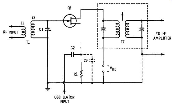
Fgr. 4-4. Mixer/converter.
mixer/converter. This is basically an amplifier circuit in which the rf input is injected at the gate of the FET (through rf transformer T1), the local oscillator signal is injected (through capacitor C2) across the usually unby passed source resistor (R1), and the i-f signal is coupled out of the drain circuit through the i-f transformer (T2). The field-effect transistor is especially effective as an rf mixer, since in this function its cross modulation (minimized by its square-law transfer characteristic) and noise figure are superior to those of either the vacuum tube or the bipolar transistor.
4.6 AF AMPLIFIER WITH AGC
Fgr. 4-5 shows the circuit of a simple audio-frequency voltage amplifier incorporating automatic gain control. This is a conventional RC-coupled arrangement to which has been added the signal rectifier circuit Dl-R5-R8. The low-voltage DC gate control feature of the FET suits it very well to age amplifier operation.
Operation of the circuit is straightforward: The output signal appearing across resistor RS is rectified by diode D1.
The resulting direct current is transmitted by filter resistor R5 to the gate of the input FET (Q1) through gate resistor
Fgr. 4-5. Audio amplifier with age.
R1 to ground. The corresponding voltage drop across R1 is in the correct polarity to reduce the gain of Q1 if diode D1 is correctly poled. With the JFET shown here, the normal gate bias is negative, so the age voltage must be positive.
When R5 is properly proportioned with respect to R1, the DC age voltage developed at the gate by diode D1 will set the optimum level for the control action. As the input-signal voltage increases, so does the output-signal voltage across RS. The DC output of D1 increases proportionately and DC creases the gain of Q1 (and accordingly that of the entire amplifier), thus reducing the output-signal voltage. It is in this way that the gain is automatically controlled.
Diode D1 should be a silicon unit, since the very high front-to-back resistance ratio of the silicon diode permits high resistances for R5 and RS. This means that RS will not adversely load the amplifier and also that good voltage divider performance may be obtained with the normally high gate resistor, R1.
4.7 CHOPPER
Numerous circuits have been designed for solid-state dc to-ac choppers. Fgr. 4-6 shows an asymmetrical circuit that uses a FET to exploit the simplicity of a single-transistor circuit.
A square-wave switching signal, supplied by generator G1 through coupling transformer T1, alternately switches the FET (Q1) on and off. This switching signal is applied between gate and source. When Q1 is ON, the DC input-signal current is conducted through Q1 and output resistor R1.
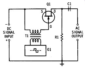
Fgr. 4-6. Chopper.
The voltage drop developed across R1 constitutes the output signal. When Q1 is OFF, the path through the FET is effectively open. Ideally, no voltage appears across R1. In effect, then, the FET acts as a fast-working electronic switch that alternately connects and disconnects R1 and the DC SIGNAL INPUT terminals.
The output-signal voltage is proportional to the DC input signal voltage, and has the frequency of the switching VOLTAGE. Common practice is to amplify the chopper-circuit out put with an ac amplifier, and then to rectify the output of the latter back to de, securing in this way the desired DC voltage amplification without the instability so often en countered with a DC amplifier. Capacitor C1 is inserted when the chopper must be blocked from the external device.
Unbalanced circuits of this kind using bipolar transistors have often been undesirable because of their significant off set voltage (output voltage present during the OFF interval). The FET, owing to its very high resistance, permits very little leak-through, and this results in offset levels of only a few microvolts.
4.8 ELECTRONIC DC VOLTMETERS
The vacuum-tube voltmeter was never seriously challenged by any bipolar-transistorized version of itself. The reason for the poor competitive position of the transistorized instrument was the low input resistance of the bipolar, which usually restricted the sensitivity to 100,000 ohms per volt, with a different input resistance on each range. Nevertheless, many such transistorized voltmeters have been used because they offered economical, portable battery operation for the first time, and also because the input resistance is comparable to that of a vacuum-tube voltmeter on the 100-V range.
Now the FET permits transistorization of the voltmeter, with all of the advantages of the VTVM ( constant input resistance--e.g., 11 megohms-on all ranges, linear DC response, and low drift) plus independence from the power line, and low battery drain. Fgrs. 4-7 and 4-8 show FET electronic DC voltmeter circuits. The exact correspondence with equivalent VTVM circuits is easily seen.
A single-FET (unbalanced) circuit is shown in Fgr. 4-7.
Like its tube counterpart, this circuit needs to be reset to zero oftener than the conventional balanced circuit does. However, its zero drift is slight and very slow, and the circuit response is linear. The simplicity of this circuit is noteworthy.
The total resistance of the input-signal voltage divider ( R1 to R4) commonly is 10 megohms. An additional 1-meg ohm isolating resistor in the DC probe brings the input resistance of the instrument up to 11 megohms on all ranges.
However, this resistance may be increased, if desired, especially if a MOSFET is employed (100 megohms input is not unusual). While 1-, 10-, 100-, and 1000-V ranges are shown here, intermediate ranges also are often provided: e.g., 0.3, 3, 30, 300, and 3000 V. Resistor R5 introduces no voltage drop, but with capacitor C1 forms a simple input filter for removing stray ac signals that may be picked up by the input circuit of the instrument.
Potentiometer RS is the conventional zero-set control, and rheostat R6 is the calibration control that allows meter M1 to be set initially to full scale with a standard DC input VOLTAGE, such as 1 V. The zero-set operation consists of balancing the drain-circuit bridge whose four arms are R7, the internal drain/source resistance (rD) of the FET, and the two halves of R8.
Isolating Resistor In Probe
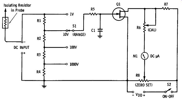
Fgr. 4-7. Electronic DC voltmeter (single-ended).
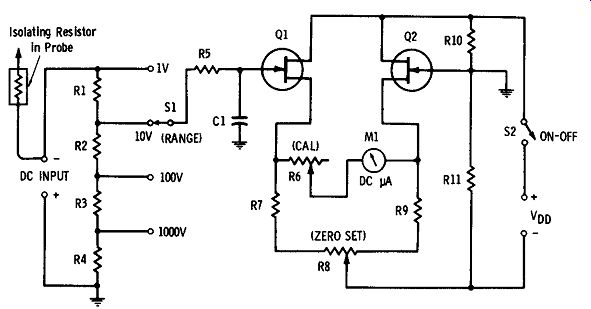
Fgr. 4-8. Electronic DC voltmeter (balanced).
An input shunt-diode probe will adapt the instrument to ac voltage measurement, but a special calibration of meter M1 then will be needed, owing to the nonlinearity of the diode at low voltages.
Fgr. 4-8 shows a two-FET (balanced) circuit. Like its tube counterpart, this circuit has almost no zero drift; and once potentiometer RS is set to zero microammeter Ml, it seldom needs resetting. Also, the circuit is remarkably free from the effects of varying FET parameters.
As in the equivalent tube circuit, the total resistance of the input-voltage divider ( R1 to R4) commonly is 10 meg ohms, and an additional 1-megohm isolating resistor in the DC probe brings the input resistance of the instrument up to 11 megohms on all ranges. However, this resistance may be increased, if desired, especially if a MOSFET is employed (100 megohms input is not unusual). While 1-, 10-, 100-, and 1000-V ranges are shown here, intermediate ranges also are often provided: e.g., 0.3, 3, 30, 300, and 3000 V. Resistor R5 introduces no voltage drop, but with capacitor C1 forms a simple filter for removing any stray ac signals that may be picked up by the input circuit of the instrument.
Potentiometer RS is the conventional zero-set control, and rheostat R6 is the calibration control that allows meter M1 to be set initially to full scale with a standard input voltage, such as 1 V. The zero-set operation consists of balancing the drain-circuit bridge whose four arms are more complicated than those in the one-FET circuit ( Fgr. 4-7). Fgr. 4-9 shows the equivalent bridge of the two-FET circuit. Here, ro1 and ro2 are the internal drain/source resistances of FET's Q1 and Q2, respectively. The four arms of the bridge are:
Arm 1 = r01 , Arm 2 = R7 + Rx, Arm 3 = ro2 , Arm 4 =
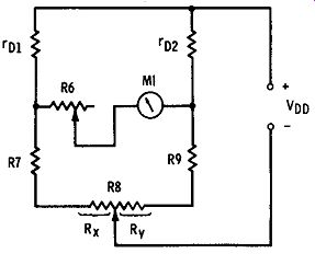
Fgr. 4-9. Equivalent zero-set bridge.
An input shunt-diode probe will adapt the instrument to ac voltage measurement, but a special calibration of meter M1 will be needed, because of the nonlinearity of the diode at low voltages.
4.9 ELECTRONIC AF VOLTMETER
A standard design for an electronic voltmeter for measuring af volts and millivolts (down to 1 mV full scale) consists of a high-gain af amplifier followed by a rectifier-type DC meter. There are many vacuum-tube voltmeters of this type. Fgr. 4-10 shows a FET version of this useful instrument.
The FET af amplifier provides the necessary voltage stepup from low input-signal voltages. The amplifier output signal voltage is transmitted to the rectifier-type meter circuit (Dl-D2-R5-Ml) through blocking capacitor C2. The amplifier gain must be high enough to raise the lowest desired input-signal voltage to the level required to deflect M1 to full scale (2.5 V rms deflects a 0-100 DC microammeter to full scale when D1 and D2 are 1N34A germanium diodes, C2 = 0.02 µ,F, C3 = 1 µ,F, and R5 = 0). In the meter circuit, rheostat R5 is the calibration control that permits M1 to be set to full scale with a standard af input voltage (at the AF INPUT terminals), e.g., 1 V. The total resistance of the input-signal voltage divider ( R1 to R4) commonly is 10 megohms, although in some commercial instruments it is as low as 1 megohm. However, this resistance may be increased, if desired, especially if a MOSFET is in the first stage of the amplifier. The range taps are unlabeled in Fgr. 4-10, but common input-signal voltages for full-scale deflection are 1, 3, 10, 30, 100, and 300 mV; and 1, 3, 10, 30, 100, and 300 V. Blocking capacitor C1 protects the instrument from any DC component in the input signal.
For wide frequency response (most vacuum-tube volt meters of this type operate up to 1 MHz), the amplifier must be properly compensated. The method, employing compensating inductors and selected drain and source resistor values, is essentially the same as that used in the design of tube-type video amplifiers.
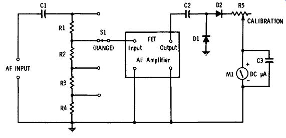
Fgr. 4-10. Electronic audio-frequency voltmeter.
4.10 INTERVAL TIMER
The use of a field-effect transistor in a simple RC-type electronic timer is completely successful, since the FET gate, like the vacuum-tube grid, does not load the timing capacitor. Fgr. 4-11 shows a timer circuit of this kind. In this arrangement, the time interval during which the relay (RY) remains closed is determined by capacitance C1 and resistance R1 (t = I0-6 RC, where t is in seconds, R is in ohms, and C is in microfarads). Since R1 is a rheostat, this resistance may be calibrated and subsequently set to any desired time value within the R1- C1 range. Switch S1 (usually a pushbutton) is a single-pole double-throw unit normally closed in position B. When S1 momentarily is thrown to position A, capacitor C1 charges almost instantaneously from battery Bl. When S1 is allowed to return to position B, the capacitor discharges through resistance R1 in RC seconds. The voltage of battery B1 must not exceed the gate/ source bias voltage developed by drain current in source resistor R2.
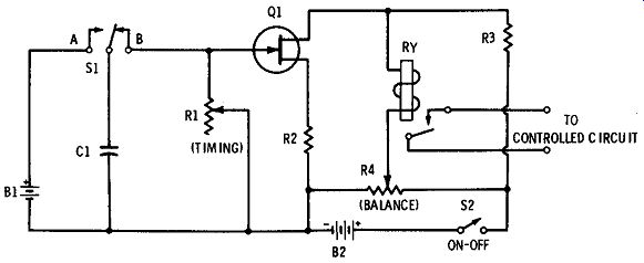
Fgr. 4-11. Interval timer.
Relay RY is a sensitive DC unit (usually 1-mA pickup)
that is connected in a bridge circuit in the FET output so that the steady drain current may be balanced out of its coil. The four arms of the bridge consist of rv ( the internal drain/source resistance of FET Q1), resistor R3, and the two halves of balancing potentiometer R4. When S2 first is closed, if R4 is not accidentally in balance, the FET drain current will pick up the relay. The adjustment of R4 then balances the bridge and reduces the relay-coil current to zero; the relay accordingly drops out (just as adjusting the zero-set potentiometer in an electronic voltmeter circuit zeroes the meter) . The timer then is ready to operate.
The operation consists of closing S1 momentarily to position A and then releasing it to return to position B. This causes C1 to charge from battery B1 and then to apply a positive voltage to the gate of Q1. This reduces the negative bias already present at the gate, and increases the drain current. The bridge accordingly unbalances, and the relay is picked up. Meanwhile, capacitor C1 discharges slowly through R1, and when it has discharged sufficiently, the original negative gate-voltage value will be re-established; the drain current will decrease and the relay will drop out.
4.11 FLIP-FLOP
There are many circuits for solid-state flip-flops; some of them are highly sophisticated. Fgr. 4-12 shows the basic circuit, here employing a pair of JFET's ( Q1 and Q2).
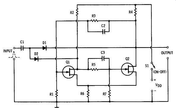
Fgr. 4-12. Flip-flop.
The bistable mode of operation of this flip-flop is identical with that of the equivalent tube circuit: The FET's are either conducting or nonconducting; when Q1 is ON, for example, Q2 is OFF. The "ON" FET automatically switches the other FET "OFF," and vice versa. Whichever FET is ON will remain ON until it is switched off by means of an actuating signal, or until the V DD DC supply is shut down; likewise, whichever FET is OFF will remain OFF until it is switched on by an actuating signal, or until the V DD dc supply is shut down. This switching back and forth between the two FET's is accomplished by means of a sharp positive pulse injected at the INPUT terminals. The output of the flip-flop is connected to the drain of Q2; but this FET is ON only half of the time, which means that the number of output pulses in a given interval of time is one-half the number of input pulses. The flip-flop therefore is a scale-of-2 frequency divider.
The operation of the circuit shown in Fgr. 4-12 starts when the on-off switch, S1, is first closed. Drain current then exists in both FET's, but a transient pulse, caused by the switch closure or by random noise, drives the gate of one FET, momentarily causing the drain current of that FET to exceed the drain current of the other one. If, for illustration, the affected FET is Q1, the increased drain current raises the voltage drop across resistor R2, thereby lowering the drain voltage of Q1. This fall in voltage is transmitted through the voltage divider R5-R7 to the gate of Q2, and lowers the Q2 drain current, increasing the Q2 drain voltage. This higher drain voltage is transmitted back to the gate of Q1 through voltage divider R3- R1, and raises the Q1 drain current still further. This sequence of actions becomes cumulative in effect, until Q1 is fully conducting (drain current maximum) and Q2 cut off (drain current zero or a very low minimum). This then is one of the two stable states of the circuit: Q1 ON, Q2 OFF. When a pulse is applied to the INPUT terminals so as to make the top terminal positive, diodes D1 and D2 transmit this pulse simultaneously to both drains. The pulse acts to increase drain current momentarily, but the drain current of Q1 is already maximum (saturated), so the pulse has no effect on this FET. Since Q2 is cut off, the pulse momentarily increases its drain current, increasing the voltage drop across R4 and lowering the Q2 drain voltage. This decrease in voltage is transmitted, through voltage divider R3- R1, to the gate of Q1, and this results in a lowering of the Q1 drain current. The action now proceeds rapidly in this new direction until finally Q1 is cut off and Q2 is fully con ducting. This then is the second of the two stable states of the circuit: Q1 OFF, Q2 ON.
The next input pulse switches Q1 ON again, and switches Q2 OFF. Thus, one output pulse (Q2 ON) is delivered for every second input pulse. The alternate switching action is rapid.
While FET's of any type are usable in flip-flops, special switching FET's give highest-speed operation (the switching time of Type 2N4351, for example, is 270 ns).
4.12 CAPACITANCE RELAY
Its very low gate/source capacitance fits the MOSFET very well for use in the oscillator section of a capacitance relay. This type of relay is well known as a proximity DC vice, because of its industrial, domestic, and entertainment applications.
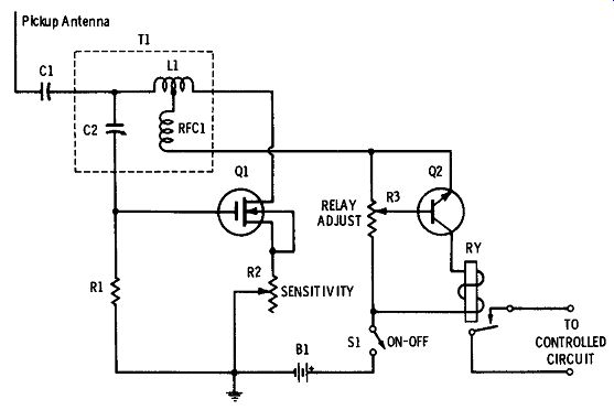
Fgr. 4-13. Capacitance relay.
Fgr. 4-13 shows a conventional circuit in which the usual vacuum-tube oscillator has been replaced with a MOSFET ( Q1), and the usual gas-type relay tube has been replaced with an npn bipolar transistor (Q2). Assembly T1 is a commercial capacitance-relay "coil," which contains the tapped oscillator inductor L1, trimmer capacitor C2, and rf choke RFC1. The source resistor (R2) is a wirewound rheostat for controlling oscillator sensitivity, and the drain resistor (R3) is a wirewound potentiometer for adjusting the pickup point of the relay. The relay itself (RY) is a single-pole single-throw, normally open, sensitive DC type (usually 1 or 2 mA). When on-off switch S1 is closed, the Q1 circuit usually will oscillate if no conductive objects are near the pickup antenna and if rheostat R2 is set near the center of its resistance range. Also, relay RY will probably close, and R3 must be set to the point at which the relay just drops out.
If the operator's hand then is held close to the antenna, his body capacitance will throw the circuit out of oscillation, the Q1 drain current will rise, and the voltage drop across R3 will increase. The base of Q2 will receive an increased DC voltage, and the relay will close. When the hand is with drawn, the circuit resumes oscillation and the relay again drops out.
By adjustment of the sensitivity control rheostat (R2) and the oscillator trimmer capacitor (C2), the circuit may be made more or less sensitive, as desired, for operation by objects at some desired distance from the antenna.
Since transistors like Q1 are low-powered devices, a capacitance relay incorporating them is less apt to create radio interference than is one using tubes operated, as they are, at 100 V or higher.