When the bipolar transistor first appeared, it caused circuit designers almost endless frustration. These specialists, long accustomed to the vacuum tube, found the low input impedance and the current dependence of the transistor un congenial factors. Some of the new problems confronting them included stepdown coupling transformers that wasted some of the voltage gain of a preceding stage while affording a power gain, the need for additional stages in an RC coupled amplifier for a given overall voltage gain, and some what inferior input/output isolation. Special components, such as af and i-f transformers, size-compatible with the transistor, eventually became available and put an end to the improvising that had become a necessary part of transistor experimenting. Even then, however, the transistor had to be constantly thought of in terms of current amplification and power gain.
Undoubtedly, had the field-effect transistor come first, the changeover from tubes would have been less painful.
In the years since the birth of the bipolar transistor, how ever, an entire generation of new engineers has come of age, and many of them have had most of their experience with transistors, not tubes. It seems pointless, therefore, to say to them that the FET will once again allow them to think very much along tube lines when they design circuits. In stead, it seems sufficient to present basic FET design data here, making comparisons with comparable tube and bipolar-transistor circuits where appropriate.
This section offers some elementary design and application data selected to acquaint the newcomer further with the FET. Illustrative examples, showing each step in calculation, are offered for the benefit of the student. For simplicity, an N-channel JFET is shown in the schematics (the V nn polarity is also correct for a P-channel depletion-type MOSFET). However, this JFET may be replaced in the circuits with a P-channel JFET if the polarity of V_dd is reversed. In all equations, current is given in amperes, VOLTAGE in volts, resistance in ohms, and transconductance in mhos (multiply by 10^-6 the g_fs value given in micromhos in the FET manufacturer's data sheet).
3.1 DC BIAS AND CIRCUIT RESISTORS
Like its tube and bipolar counterparts, a FET is operated at a selected point on its response curve, determined by DC bias levels. Fgr. 3-1A shows a common-source circuit with the currents, voltages, and resistors involved (since gate/ source current is virtually zero, for practical purposes, it is ignored in the equations, so source current Is becomes identical with drain current In). Fgr. 3-1B shows a similar source-follower circuit.
Common-Source Circuit
Suppose that it has been determined from the FET curves that Class-A amplifier performance requires FET Q1 ( Fgr. 3-1A) to be operated at Vns = 8 V, In= 0.5 mA, and V Gs= -2 V. Suppose further that the available battery voltage Vnn = 22.5 V. The value of source resistor Rs required for V Gs = -2 is:
Rs= VGs/lo
= 2/0.0005 = 4 k-ohm
The value of the drain resistor RL is: R
_ Yoo - (Vos+ loRs)
L - Io R _ 22.5 - [8 + 0.0005 ( 4000)] L - 0.0005
_ 22.5 - (8 + 2)
0.0005
= 12.5/0.0005 = 25 k-ohm (3-1)
(3-2)
Another aspect of the problem of biases and resistors concerns an assigned value of RL,
For example, an RL value of 62 k-ohm is specified, since it is twice 31 k-ohm, the input resistance of a succeeding stage in a particular amplifier circuit. For the same FET given in the preceding example, V oo must be determined (Rs will be the same 4 k-o, since the required V Gs still is -2 V, and drain current Io still is ...
(A) Common source. (B) Source follower.
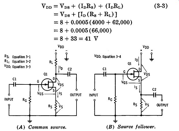
Fgr. 3-1. DC voltages.
Source-Follower Circuit
The bias situation is somewhat different in the source follower circuit ( Fgr. 3-1B), since this circuit has no drain resistor. Source resistor Rs serves as the output resistor, as well as the source of automatic gate bias.
As in the common-source circuit, it is desirable here to operate the FET at a point that will assure Class-A performance. Usually, since Rs will be chosen beforehand for a desired output impedance, the supply voltage must be determined for the specified value of drain current.
Example: Suppose Rs is chosen as 10000, and the FET must operate at VDs = 12 V, ID= 1 mA, and VGs = -1 V. If Equation (3-1) is rewritten VGs = IDRs, then the gate bias voltage here is V Gs= 0.001 (1000) = 1 V, which was required. The required supply voltage is calculated:
VDD = VDs + IDRs
= 12 + [0.001 (1000)]
= 12 + 1 = 13 V (3-4)
Source resistor Rs has the dual function of supplying automatic gate bias to the FET and establishing the output impedance of the circuit at the same time. But it sometimes fails to perform both functions satisfactorily. For example, suppose that Class-A performance demands that the FET be operated at V Ds = 12 V, In= 1 mA, and V Gs= -1 V, and that Rs must be 500 ohms. Equation (3-1) rewritten shows now that V Gs = 0.001 ( 500) = 0.5 V ( only one-half of the required gate voltage). The additional 0.5 V would have to be provided by a supply connected between the bottom of resistor RG and ground if, as assumed, neither Rs nor In may be changed. Conversely, if the voltage drop IDRs exceeds the required gate-bias value, the bottom of resistor RG must be connected to a point along Rs that will provide the correct voltage division.
Gate Resistor
In all of the examples, the gate resistor (RG) may be chosen arbitrarily. As in a tube circuit, but not a bipolar transistor circuit, this resistance may be high ( too high a value will make the circuit oversensitive to noise and stray signals); a common value is 1 to 20 megohms.
3.2 COMMON-SOURCE AMPLIFIER (BYPASSED Rs)
Fgr. 3-2 shows the circuit of a single-stage, common source, small-signal amplifier. Here, as in the common cathode tube circuit, the source resistor (Rs) is bypassed (by C2). Thus, the circuit, lacking degeneration, is capable of its highest amplification under a given set of operating conditions.
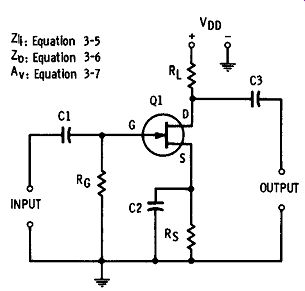
Fgr. 3-2. Common-source amplifier (bypassed Rs), Input Impedance
Equation 3-5
Equation 3-6
Equation 3-7
In this circuit, the input impedance is determined by gate resistor R_G :
Z_1=R-G (3-5)
This convenient attribute places the input impedance of the circuit completely in the hands of the designer. In most practical instances, the gate/source resistance of the FET is enormous in comparison with any values of R_G commonly chosen.
Output Impedance
The output impedance is equal to the value of load resistor RL, Sometimes, this resistance may be chosen arbitrarily; often, however, it will be better determined by means of Equation (3-2). In any event, (3-6)
Voltage Gain
The open-circuit voltage amplification of the circuit may be calculated: (3-7)
Example: A Type 2N3631 MOSFET with typical trans conductance of 2000 µmho is operated with a drain resistor (Rd of 10,000 !l. The expected voltage gain A,.=
0.002(10,000) = 20.
3.3 COMMON-SOURCE AMPLIFIER (UNBYPASSED Rs)
If bypass capacitor C2 is omitted in Fgr. 3-2, the unby passed source resistor (Rs) will give rise to current degeneration, which serves to reduce distortion and to linearize response. But its action also reduces the voltage gain.
Input Impedance Here, as in the original circuit with the bypassed source resistor, the input impedance is determined by gate resistor RG: (3-8)
Resistance RG is held to 1 to 20 megohms in most practical circuits, to minimize noise and stray signal pickup.
Output Impedance
The output impedance, as in the preceding example, is equal to the load resistor value. Sometimes, this resistance may be chosen arbitrarily; often, however, it will be determined by means of Equation (3-2). In any event, (3-9)
Voltage Gain
The open-circuit voltage amplification of the circuit may be calculated: (3-10)
Example:
A Type 2N2608 JFET (typical transconductance= 1600 µmho) is operated with RL = 20 k-ohm and Rs= 1.6 k-Ohm. The voltage gain is:
0.0016 (20,000) Av= 1 + [0.0016 (1600)] 32 1 + 2.56
= 32/3.56 = 8.98
Note that if the source resistor is bypassed, and the amplification accordingly is calculated by means of Equation (3-7), A,= 32, or 3.56 times the unbypassed value.
Fgr. 3-3. Source follower.
3.4 SOURCE FOLLOWER
Fgr. 3-3 shows the circuit of a source follower. Like the tube-type cathode follower and bipolar-transistor-type emit ter follower, this circuit has many applications as a high impedance to low-impedance converter with power gain.
Input Impedance
In this circuit, the input impedance is determined by gate resistor RG :
(3-11)
Resistance RG is held to 1 to 20 megohms in most practical circuits, to minimize noise and stray signal pickup.
Output Impedance
The output impedance may be calculated:
z _ Rs
0
-1 + gr. Rs (3-12)
Example: When a Type 2N2609 JFET (transconductance= 3600 µmho, typical) is operated in the circuit in such a way that VDs = 15 V, los = 1 mA, and VGs = 0.5 V, Rs must be 500 n. The output impedance is :
500 Zo = 1 + 0.0036 (500) 500 1 + 1.8
= 500;2.8 = 178.6 n
Voltage Gain
The open-circuit voltage amplification of the circuit may be calculated : A - gr. Rs (3-13)
v - 1 + gr. Rs
Example: Use the instance of the 2N2609 JFET source follower cited in the preceding calculation of output impedance. The voltage amplification is:
As with the cathode follower and emitter follower, the VOLTAGE "gain" of the source follower is less than 1.
3.5 BOOTSTRAP CIRCUIT
Fgr. 3-4 shows the circuit of a specialized source follower that is useful for increasing the typical input impedance of a JFET beyond the 109-ohms maximum mentioned in Chap ter 1. It takes its name from the fact that such a circuit seems to lift the input impedance by its own bootstraps.
VGS:
Equation 3-14
Z I : Equation 3-15 Zo: Equation 3-16 Av: Equation 3-17 C1
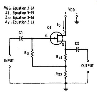
Fgr. 3-4. Bootstrap circuit. r RG
In this arrangement, the source resistor consists of two series-connected elements (Rs1 and Rs2), and the gate resistor (R0 ) is returned to their junction. The Vos bias VOLTAGE required for correct operating point of the FET is the voltage drop developed across Rs1 by drain current ID:
Vos= loRs1 (3-14)
Example: Suppose a 2N2609 JFET (transconductance= 3600 µmho, typical) is to be operated at VDs = 15 V, IDs= 1 mA, and Vos= 0.5 V.
Rewrite Equation (3-14), Rs1 =Vos/ ID = 0.5/0.001 = 500 ohm. This will be the required value for the top member of the source-resistor combination.
The lower half (Rs2) of the combination must be chosen as high as the supply voltage (V DD) will permit, in order to keep the voltage gain as high as possible. If the Rs2 value is selected as 10 k-ohm, the total source resistance (Rs1 + Rs2) is 10,500 0, and this necessitates a drain supply (V DD) of 10.5 V. Input Impedance The approximate input impedance of the bootstrap circuit may be calculated:
z1
= RG(Rs1 + Rs2)
Rs1 (3-15)
Example: Assume that the gate resistor (RG in Fgr. 3-4)
is 1 megohm. Then Z1 equals :
Output Impedance z _ 106 (500 + 10,000) i- 500
- 10^6 (10,500) 500
= 1.05 (108) = 21 MO 5
The output impedance may be calculated: z _ Rs1 + Rs2
0
- 1 + gfs (Rs1 + Rs2)
(3-16)
Example: For the same JFET and the values given in the preceding discussion,
Voltage Gain
500 + 10,000 Zo = 1 + 0.0036 (500 + 10,000) 10,500 1 + 0.0036(10,500)
_ 10,500 1 + 37.8
= 1
~:,~o = 210.6 ohm
For the same JFET and the values given previously, the open-circuit voltage amplification may be calculated:
A _ gr. (Rs1 + Rs2)
v - 1 + gr. (Rs1 + Rs2)
0.0036 ( 500 + 10,000) 1 + 0.0036 ( 500 + 10,000)
_ 0.0036 (10,500) 1 + 0.0036 (10,500) 37.8 37.8 O 974 1 + 37 .8 = 38.8 = .
3.6 FET/BIPOLAR CASCADE
(3-17)
In some impedance-transforming amplifiers, a FET is direct-coupled to a bipolar transistor. This arrangement (see Fgr. 3-5) gives the circuit the high input impedance of the FET, and somewhat higher gain and lower output impedance than are afforded by a conventional source follower.
Voo
+ -
Z 1: Equation 3-18
Zo: Equation 3-19
Av: Equation 3-20
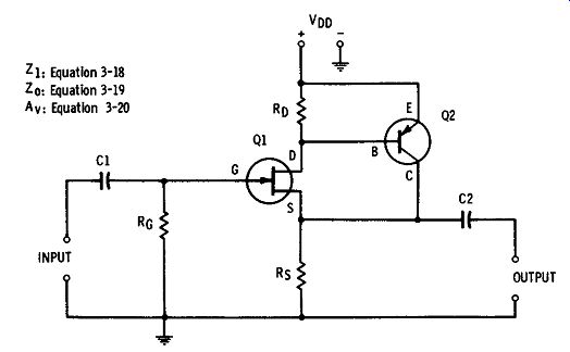
Fgr. 3-5. FET /bipolar cascade.
For a practical example of this application, let the FET (Q1) be a Type 2N2608 JFET (transconductance= 1600 µ,mho, typical) and the bipolar transistor (Q2) be a 2N525 pnp unit (hre = 30, h1e = 1400 ohm). For the resistors, RG = 5 M-ohm, RD = 20 k-ohm, and Rs = 1.6 k-o. These values will be used in the illustrative examples that follow.
Input Impedance The input impedance is equal to the resistance of the gate resistor: (3-18)
Output Impedance The output impedance may be calculated: z _ Rs
0
-1 + gr.Rs (3-19)
Example: For the semiconductors and the values given above: 1600 Zo = 1 + 0.0016(1600) 1600 1 + 2.56
= 1~;~ = 449.4 ohm
Voltage Gain The open-circuit voltage amplification may be calculated: A
_ gr. Rs [ hre (Ro ~~\J] v- R 1 + gr. Rs[ hre( Ro : hJ] (3-20) Example: Use the semiconductors and the circuit values given in the preceding discussion:
[ ( 20,000 )]
0.0016(1600) 30 20 000 + 1400 Av= , 20 000 1 + 0.0016(1600)[ so( 2o,ooo' + 1400)] 2 56[3o( 20,000)]
. 21,400 1 + 2 56[30(20,000)]
. 21,400
2.56[30 (0.935)]
-1 + [2.56(30)0.935] = 71.
31
= 0 986 72.81.
Note that for this circuit, the voltage gain is close to unity (being only 1.4 percent lower), whereas Av for the straight source follower (Section 3.4) was 0.643, and Av for the bootstrap circuit (Section 3.5) was 0.974.
3.7 FET CAPACITANCE
The capacitances of a field-effect transistor are usually so low that they often may be neglected in many circuit calculations. MOSFET input capacitance is very low. In certain instances, however, such as operation at vhf and uhf frequencies, FET capacitances must be considered, since they then become significant components of device impedances.
Gate Drain ros INPUT OUTPUT Source
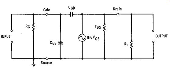
Fgr. 3-6. Equivalent circuit of common-source amplifier.
In Fgr. 3-6, the equivalent circuit of the common-source amplifier, the positions of the FET input capacitance (internal gate/source capacitance CGs) and feedback capacitance (internal gate/drain capacitance CGo) are shown. In this circuit, RG represents the external gate resistor, RL is the external drain (load) resistor, ros is the internal drain/ source resistance of the FET (rvs =Vos/Io), and the equivalent internal generator is represented by its effect gr. V Gs. Feedback capacitance CGD is equivalent to the grid/plate capacitance of the vacuum tube, and like the latter must be neutralized in some FET amplifiers. In metal-cased FET's, additional capacitances are present between gate and case, drain and case, and source and case [sometimes, one electrode (e.g., the gate) is internally connected to the case, and the corresponding capacitance between that electrode and case is eliminated]. Because the FET is a relatively high-gain triode with internal feedback capacitance (CGo), it is subject to the Miller effect, which acts to multiply the input capacitance (CGs). The Miller effect accordingly must be taken into account in all applications (e.g., tuned amplifiers) and in all precise calculations of input impedance (or admittance) or amplifier phase shift.