While all varactor applications ultimately are based on voltage-sensitive
capacitance, the particular ability of the varactor to tune circuits, provide
adjustable reactance, and generate harmonics makes it useful in transmitters.
Some of its practical functions include oscillator and amplifier-tank tuning,
frequency multiplication, frequency modulation, amplitude modulation, and output
control.
The varactor has greatly simplified some modern transmitters, especially lightweight, portable units and remote controlled sets. In this role, it has also provided noteworthy economies-some in initial cost and others in operating expenses. In some instances, particularly in frequency multiplication, its high efficiency ( compared with that of tubes and transistors) distinguish the varactor.
TANK TUNING
The varactor may be used in lieu of, or in conjunction with, a conventional variable capacitor for tuning the LC tank of an r-f oscillator or amplifier. In this application, the r-f signal impressed across the varactor must be maintained at a voltage that will not override the DC tuning voltage and which (if important in a particular case) will not cause excessive harmonic generation.
Single-Ended Tank, Single-Varactor-Tuned
The basic LC tank-tuning circuits are shown in Fig. 4-1.
Fig. 4-1A shows a typical single-ended tank. Only one varactor is used. Here, the frequency is determined by the inductance of coil L1 and the capacitance of varactor X1. If the varactor is to account for only part of the capacitance, handset capacitor C2 may be used. C1 is a protective DC blocking capacitor. Isolating resistor R1, radio-frequency choke L2, and bypass capacitor C3 form an r-f filter to isolate the DC tuning-voltage source from the tank. If the tank is grounded directly, as shown in Fig. 4-1A, the positive terminal of the tuning-voltage supply likewise will be grounded. If, instead, the tank is r-f-grounded only (through a bypass capacitor), the tuning-voltage supply will be above ground and will require special insulation.
Single-Ended Tank, Balanced-Varactor-Tuned
Fig. 4-1B shows balanced (two-varactor) tuning of a single-ended tank. The merits of the balanced circuit were discussed in a previous section. Because the matched varactors X1 and X2 are connected in series, the total capacitance is one-half that of one varactor. The frequency is deter mined by the inductance of L1 and this total capacitance. If, however, the varactor pair is to account for only part of the capacitance, a handset capacitor ( C1) may be used. C2 is a protective DC blocking capacitor. Isolating resistor R1, r-f choke L2, and bypass capacitor C3 form an r-f filter, as in the preceding circuit. Here, as before, if the DC tuning voltage circuit is above ground, it will need special insulation unless coil L1 is directly grounded, as shown.
Push-Pull Tank, Single-Varactor-Tuned
Fig. 4-1C shows a push-pull tank, each half of which is tuned by a single matched varactor ( X1 and X2). The varactors thus simulate a split-stator tuning capacitor, each receiving the DC tuning voltage at the same time through resistors R1 and R2 and the r-f filter (C5-L3). If the varactors are to account for only part of the capacitance across...
(A) Single-varactor, single-ended. (B) Balanced-varactor, single-ended.
(C) Single-varactor, push-pull.
(D) Balanced-varactor, push-pull.
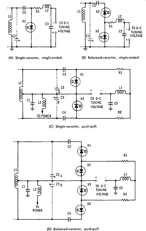
Fig. 4-1. Tank-tuning methods.
...tank coil L1, a split-stator handset capacitor (C3) may be used. C2 and C4 are protective DC-blocking capacitors. The "series-fed" tank circuit, common in transmitters in the form shown here, is r-f grounded through capacitor C1 but is not grounded for direct current. The DC tuning-voltage source therefore is above ground and needs special insulation. A "shunt-fed" tank, on the contrary, has the center tap of coil L1 grounded (the transmitter stage receiving its direct current through an r-f choke and delivering r-f energy to. the tank through a blocking capacitor) and avoids this difficulty.
Push-Pull Tank, Balanced-Varactor-Tuned
The advantages of balanced-varactor tuning are available also in push-pull tanks, provided no objection exists to using four matched varactors. Fig. 4-1D shows a balanced varactor push-pull tank. Note that the arrangement on one side of the center tap of coil L1 is a mirror image of that on the other side, and that each side is a duplicate of the balanced single-ended tank shown in Fig. 4-1B, except for the sharing of a single r-f choke and bypass capacitor (L3 and C5 in Fig. 4-1D). In Fig. 4-1D, varactors X1 and X2 simulate one section of a split-stator variable capacitor, and X3 and X4 simulate the other section. The total capacitance of X1 and X2 in series equals the total capacitance of X3 and X4 in series; however, each total capacitance, because of the series connection of the constituent varactors, is one-half the capacitance of one varactor. If the varactor combination is to account for only a part of the tank capacitance, a split stator handset capacitor (C3) may be used. As in the pre ceding example, a common series-fed tank is shown here.
This arrangement is r-f-grounded through bypass capacitor C1 but has no DC ground. The DC tuning-voltage source is therefore above ground and needs special insulation. In a shunt-fed tank, however, the center tap of coil L1 is grounded and the DC voltage is supplied through an r-f choke past a blocking capacitor, eliminating this problem.
Oscillator Tuning
Fig. 4-2 is the circuit of a low-powered transistor r-f oscillator. Such units are used as master oscillators in multistage transmitters, or as flea-power transmitters themselves. With the constants shown, the circuit is capable of approximately 100-mw DC input power. Radio-frequency energy may be coupled out of the tank either capacitively or inductively.
Varactor X1 is shunted across tank coil L1, through protective DC-blocking capacitor C5, and acts as the tuning ...
(B) Voltage-frequency response with L1 equal to 0.4 microhenry.
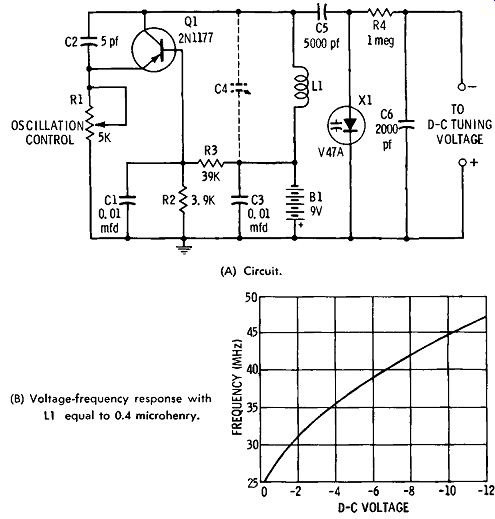
Fig. 4-2. Voltage tuning of low-powered transistor oscillator.
... capacitor. But if the varactor is to account for only part of the tank capacitance, C4 may be inserted as a handset capacitor. ( Often, instead of this capacitor, a slug-tuned coil is substituted for the air-wound one shown at L1.) Varactor X1 is chosen to supply the absolute capacitance and required capacitance range to tune L1 over the desired frequency range with the available DC control voltage. In some in stances, the oscillator supply voltage (B1) will also supply the tuning voltage through a potentiometer, greatly simplifying the transmitter.
The circuit shown will operate at any frequency up to 100 MHz if L1 is chosen to resonate with the varactor. Fig. 4-2B shows how the operating frequency may be varied between 25 and 47.5 MHz by varying the DC voltage from -0.5 to -12 volts, when L1 is 0.4 µ,h and varactor X1 is a Type V47A (nominal capacitance= 47 pf). Similar r-f oscillators are based on the tunnel diode for even greater simplicity than that of the transistor circuit; however, the power output and efficiency are lower.
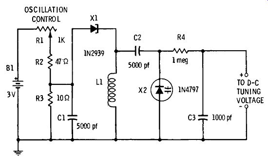
Fig. 4-3.
Voltage tuning of tunnel-diode oscillator.
Fig. 4-3 shows a varactor-tuned tunnel-diode oscillator. Here, tunnel diode X1 is operated at approximately 0.1 vdc, derived from 3-volt battery B1 through voltage divider R1, R2, and R3; the voltage is set for strongest oscillation by adjustment of R1. The frequency is determined by the inductance of coil L1 and the capacitance of varactor X2. With the 1N4797 varactor shown (nominal capacitance= 56 pf), a DC volt age range of 0.5 volt to 6 volts, and L1 equal to 4.6 µ,h, the frequency range is 7 to 11 MHz. This circuit will oscillate as high as 250 MHz if the inductance of L1 is properly chosen.
FREQUENCY MULTIPLIERS
Harmonic generation is the most important large-signal property of the varactor. It arises as a result of the pronounced distortion occurring when the varactor is operated over its entire range of nonlinear response. This property, which was introduced in Section 2, is utilized in modern, high-efficiency passive frequency doublers, triplers, quadruplers, and higher-order multipliers.
How the varactor generates harmonics may be understood by reference to Fig. 4-4A. Here, a sine-wave AC power source (generator), varactor X1, and load resistor RL are connected in series. The generator, operating at frequency /, applies a sine-wave AC voltage, Vt, to the circuit. When Vt is high enough to swing the varactor over enough of the nonlinear portion of its current-voltage curve, the current through the varactor and load resistance is highly distorted, containing not only the fundamental frequency (/) but also a number of harmonics (h). This current accordingly is designated lt+1i in Fig. 4-4A. The current produces a voltage drop Vr+1i across load resistor RL, and this voltage likewise is a mixture of fundamental and harmonic frequency components. Now, because the varactor is a reactive device, it consumes very little power (i.e., its losses are low), so most of the generator power appears in the output (load)-indicating high efficiency. We might have connected a battery, properly poled, in series with the generator and varactor to ensure that the varactor always operates at reverse voltage, but frequency multiplication is enhanced by allowing the varactor to be driven momentarily into the forward conduction mode.
The load current Ut+1i) and resulting load voltage ( Vr+1i) are mixtures of many frequencies. In transmitter practice, we are interested in single frequencies; therefore, the operation illustrated by Fig. 4-4A is of little interest other than in accounting for the ability of the varactor to generate harmonics. A single desired harmonic frequency can be extracted from the mixture by means of a suitable filter. It is to illustrate this possibility that the next two circuits are given (Figs. 4-4B and C). Fig. 4-4B is termed a series-type multiplier from the fact that the varactor is in series with the input (generator) and the output (load). Fig. 4-4C is termed a shunt-type multiplier because the varactor is in parallel (shunt) with the input and the load. In both circuits, the proper harmonic is selected by means of two selective circuits: an input filter and an output filter.
In Fig. 4-4B, the filters are high-Q parallel-resonant circuits. The input filter ( L1- C1) is tuned to the fundamental frequency (!), and the output filter (L2-C2) to the de-
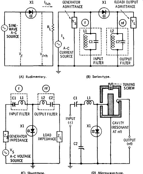
Fig. 4-4. Varactor frequency multipliers.
(A) Rudimentary. (B) Series-type. (C) Shunt type. (D) Microwave-type.
sired harmonic-or multiple off (i.e., to nf). The generator is thought of as a current source (I.) with internal admittance Y., and the output device as a load admittance, Yt.
Each of the filters offers maximum impedance at the frequency to which it is tuned; therefore, maximum voltage is developed across the filter at that frequency.
In Fig. 4-4C, the filters are high-Q series-resonant circuits. The input filter ( L1- C1) is tuned to the fundamental frequency (!), and the output filter (L2-C2) to the desired harmonic-or multiple of f (i.e., to nf). The generator is thought of as a voltage source (V.) with internal impedance z., and the output device as a load impedance, Zr,. Here, each of the filters offers minimum impedance at the frequency to which it is tuned; therefore, each allows maximum current through itself at that frequency.
Fig. 4-4D shows one version of a microwave varactor frequency multiplier. Here, capacitors C1 and C2 facilitate matching the circuit to the driving source. C1 also combines with L1 to form a series-resonant filter to pass the fundamental frequency (f) to varactor X1. The cavity is resonant at the desired harmonic ( nf) and, like the parallel-resonant filters in Fig. 4-4B, develops maximum output at that frequency. Some microwave frequency multipliers dispense with lumped constants, such as C1, C2, and L1. Instead, they employ a transmission line between the input terminals and the varactor. This line is provided with tuning stubs for resonating at frequency f.
Every varactor multiplier is some adaptation of the circuits given in Fig. 4-4. The varactor multiplier is not only efficient (i.e., P0 /P1 approaches 100 percent for doublers, where P0 is the output power, and P1 is the input power, both r-f), but it also requires no local power supply. The only power required for its operation is supplied by the input signal itself.
Doublers
The basic circuits of Figs. 4-4B and C may be used as frequency doublers simply by making n equal to 2 wherever it appears. That is, the output filter in either instance must be tuned to twice the frequency of the input signal. Fig. 4-5 shows five typical doubler circuits.

Fig. 4-5. Typical doubler circuits. (A) Simple arrangement. (B) Self-contained,
single-tuned. (C) Self-contained, double-tuned. (D) Series-resonant input
and output with wavetrap. (E) Push-push doubler.
Fig. 4-5A is a simple arrangement. Here, the L1-C1 filter is tuned to f, and L2-C2 to 2/. Noninductive resistor R1 pro vides self-bias (the varactor acts as a shunt-diode rectifier). The circuit is adapted to individual conditions by providing it with suitable input and output coupling and impedance matching.
Fig. 4-5B shows a more self-contained arrangement. In this circuit, coils L1 and L2 not only supply the inductances for the input and output filters, respectively (in conjunction with capacitors C1 and C2), but also act as impedance matching input and output autotransformers. As before, the input filter ( L1- C1) is tuned to f, and the output filter (L2-C2) to 2/. Self-bias is provided by noninductive resistor R1 (60K to 270K, depending on varactor type). In Fig. 4-5C, double tuning is employed for increased efficiency and more complete rejection of unwanted frequencies. For example, parallel-resonant circuit L1- C1 is tuned to transmit input frequency f, and parallel-resonant circuit L4-C6 to transmit output frequency 2/. Also, series-resonant circuit L2-C2 is tuned to pass f, and series-resonant circuit L3-C5 to pass 2/. Coils L1 and L4 also act as input and output autotransformers, respectively. Noninductive resistor R1 provides self-bias.
A somewhat different filtering arrangement is shown in Fig. 4-5D. Here, C1 and L1 form a series-resonant circuit which passes input frequency f to varactor X1. Following the varactor is a wavetrap-the parallel-resonant circuit, L2-C2-which serves to suppress frequency f from the out put. The output circuit contains a second-harmonic bandpass filter, the first section of which is composed of the wavetrap ( L2-C2), capacitors C3 and C5, and inductor L3; and the second section of which is composed of capacitor C4 and inductors L4 and L5. Self-bias is provided by noninductive resistor R1.
The push-push doubler is well known in tube and transistor practice and is characterized by ( 1) its use of two components to obtain double the output afforded by one, and (2) its push-pull input and parallel output. (This connection doubles power but circumvents some of the difficulties, such as increased strays and spurious responses, occasioned by straight parallel connection.). Fig. 4-5E shows a varactor push-push doubler circuit. Here, C2 and the upper half of L2 serve as a series-resonant filter to pass input frequency f to varactor X1 during one input half-cycle; C3 and the lower half of L2 perform the same function during the opposite half-cycle. Input energy is coupled into L2 through primary coil L1. which provides an impedance match to the signal source. In the output circuit, the series-resonant filter, L3-C4, passes frequency 2/ while rejecting f. Capacitor C5 aids in matching the output impedance to that of the load. Noninductive resistors R1 and R2 provide varactor self-bias.
Whereas the theoretical efficiency of tube-type doublers is given as 50 percent, this figure is obtained only through excellent design and adjustment. But the efficiency of the varactor doubler, depending on varactor type and input power, has been reported above 90 percent at frequencies as high as 100 MHz, dropping to 20 percent at 20 GHz.
Triplers
In the varactor tripler, the output filter is tuned to the third harmonic of the input signal frequency. Aside from this particular, the tripler circuit differs from the doubler circuit chiefly in its use of an auxiliary tuned circuit-the idler-to reinforce the triple-frequency output.
The basic tripler circuit is shown in Fig. 4-6A. Here, the input series-resonant filter, L1- C1, is tuned to pass input frequency f to varactor X1, and the output series-resonant filter, C3-L3, is tuned to pass the tripled frequency (3/) to the output terminals. Noninductive resistor R1 provides self bias. The idler consists of the L2-C2 leg which is tuned to the second harmonic, 2/. Second-harmonic current U2r), which flows readily through the idler, adds to the fundamental (/r) to form third-harmonic current Usr). This idler action results in higher tripler efficiency.
In Fig. 4-6B, coils L1 and L3 serve as series-resonant in put and output filter inductors (with capacitors C1 and C3, respectively), and also as input ( L1) and output (L3) auto transformers for input and output coupling and impedance matching. Here, as in the preceding example, the idler circuit is comprised of L2 and C2. Filter L1- C1 is tuned to input frequency f, L2-C2 to second-harmonic frequency 2f, and L3-C3 to output frequency 3f. Noninductive resistor R1 provides self-bias.
The only difference between Fig. 4-6C and Fig. 4-6B is the use of a tapped capacitor arrangement in Fig. 4-6C (C1-C2 at the input, and C4-C5 at the output) to provide an impedance match from the generator to the input of the tripler, and from the output of the tripler to the external load. Autotransformers are used, instead of this capacitor arrangement, in Fig. 4-6B. Coil L1 and capacitor C1 form the input series-resonant filter tuned to pass input frequency f to varactor X1, while L2 and C4 form the output series resonant filter to pass output frequency 3f to output jack J2.
Fig. 4-6. Typical tripler circuits. (A) Basic circuit. (B) Series-resonant
input and output. (C) Series-resonant with tapped capacitances. (D) Double-tuned
circuit.
Inductor L3 and capacitor C3 form the idler tuned to second harmonic frequency 2f. Noninductive resistor R1 provides self-bias.
Fig. 4-6D shows a more complicated tripler circuit using double tuning to avoid spurious responses and to improve input-output isolation. The double-tuned input consists of parallel-resonant filter L1- C1 and series-resonant filter L2 C2, both tuned to input frequency f; and the double-tuned output consists of series-resonant filter L3-C6 and parallel resonant filter L5-C7, both tuned to output frequency 3f. The idler, tuned to second-harmonic frequency 2f, consists of L4 and C4. Capacitors C3 and C5 aid in adjustment of the circuit for peak output. Noninductive resistor R1 pro vides self-bias for varactor X1.
The efficiency of varactor triplers, depending on varactor type and power input, has been reported at 60 percent at frequencies as high as 100 MHz, dropping to 5 percent at 20 GHz.
Quadruplers
All frequency multipliers beyond the doubler require an idler for maximum efficiency. If in any one of the tripler circuits (Fig. 4-6) the idler is tuned to 3f, the third-harmonic current Uar) it passes will add to fundamental current (/r) to produce fourth-harmonic current (/,+ lat= /4r). If the output filter then is tuned to 4f, the output frequency of the stage becomes four times that of the input, and a quadrupler results.
The efficiency of varactor quadruplers, depending on varactor type and input power, has been reported at 60 per cent at frequencies as high as 100 MHz, dropping to 5 per cent at 20 GHz.
Higher-Order Multipliers
Quintuplers (5x), sextuplers (6X), septuplers (7x), octuplers (8x), etc. may be made from the tripler circuits shown in Fig. 4-6, by changing the output filter to resonate at the desired harmonic, nf, and changing the idler to resonate at the frequency f ( n-1 ). Thus, the idler frequency is 4/ in a quintupler, 5f in a sextupler, 6f in a septupler, and 7f in an octupler, etc.
Efficiency decreases in high-order multipliers below that of the doubler, tripler, and quadrupler. Sometimes, better results are obtained when high-order multiplication is re quired, by cascading successive lower-order stages; for ex ample, two doublers for quadrupling, a doubler and a tripler for sextupling, etc.
FREQUENCY MODULATION
Because a varactor will tune an oscillator tank circuit, it will frequency modulate the oscillator if an audio voltage is used instead of DC voltage to vary the varactor capacitance.
Fig. 4-7 shows a frequency modulator circuit. Here, the varactor X1 is connected in parallel with the tank (L2-C4)
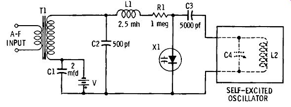
Fig. 4-7. Frequency modulator.
OSCILLATOR
of a self-excited oscillator through a protective DC-blocking capacitor, C3. With the DC bias voltage, V, adjusted to place the operating point of the varactor within a straight portion of its response curve, C4 is tuned to set the oscillator to the desired carrier (center) frequency, fb•
If an audio signal then is applied to the AF input terminals, the AF voltage at the secondary of transformer T1 will alternately aid and buck the DC voltage, increasing and decreasing the net varactor voltage. Thus, on one AF half-cycle, when the lower secondary terminal of T1 is positive, the varactor voltage will increase, the varactor capacitance will decrease, and the oscillator frequency will increase from its center value (lb) to le•
When the AF cycle passes through zero, only the DC voltage ( V) will be present at the varactor, and the oscillator frequency will return to f b•
On the opposite AF half cycle, when the lower secondary terminal is negative, the varactor voltage will decrease, the varactor capacitance will increase, and the oscillator frequency will decrease from the center value (th) to / 0 •
As the AF signal continues to go through its alterations, the oscillator frequency will swing above and below the carrier value and frequency modulation of the oscillator output will occur. If the DC operating point is within the straight portion of the varactor response curve, the frequency upswing will equal the downswing. For linear modulation, the linear portion of the curve must be used.
The modulation rate (number of frequency swings per second) is identical with the audio modulating frequency, while the sweep width (total kHz or MHz covered in the sweep) is proportional to the peak amplitude of the AF volt age. By properly proportioning the AF voltage with respect to a given r-f oscillator frequency, either narrow-band or wide-band frequency modulation may be obtained. Any of the small varactors (20- to 68-pf nominal capacitance) may be used.
AMPLITUDE MODULATION
A c-w transmitter may be amplitude modulated externally by means of the varactor-tuned antenna coupler ( L1, L2, C1, and X1) shown in Fig. 4-8A. This coupler is tuned to the carrier frequency by varactor X1, the capacitance of which may be varied by adjusting potentiometer R2 to control the varactor DC bias. The inductance of L2 and the bias voltage are chosen so that the operating point is within the straight portion of the r-f voltage vs. DC bias curve (Fig. 4-8B) for the particular varactor used. Blocking capacitor C1 keeps L2 from short circuiting the DC bias, and its reactance is negligible in tl').e circuit. L1 is a link-coupling coil.
The AF modulating voltage is applied in series with the DC bias, by means of transformer T1, which has a 2 :1 or 3: 1 step-up turns ratio. Because of the extremely high resistance of the varactor, virtually no audio power is required, and the modulating voltage accordingly may be obtained from a one- or two-stage transistor speech amplifier or directly from a carbon microphone.
Fig. 4-8B shows operation of the circuit. Note that the circuit is tuned to the high-frequency side of resonance, by adjusting the DC bias to the level Ede•
The AF voltage (Ear)
is superimposed on Ede
This causes the bias to swing above and below Ede at the audio-frequency rate. The resulting voltage across L2 therefore has the amplitude-modulated shape shown by the output pattern in Fig. 4-SB. For correct operation, R2 is set for best linearity of modulation, and the AF amplitude for desired percentage of modulation.
(B) Performance.
(A) Circuit.
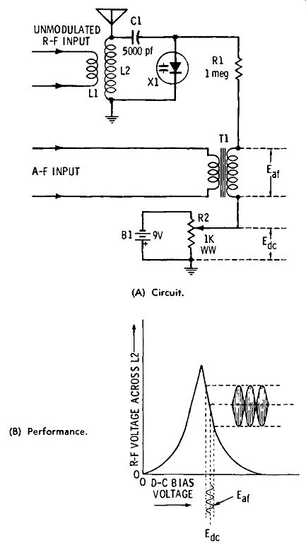
Fig. 4-8. Amplitude modulator.
RF OUTPUT CONTROL
The DC-variable reactance of a varactor may be used conveniently to vary the r-f output of a transmitter or ex citer. The varactor is connected as a variable coupling capacitor between stages, as shown between the plate tank ( L1- C1) of one stage and the grid tank (L2-C3) of the following stage in Fig. 4-9.
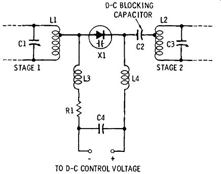
Fig. 4-9. R-f output control.
A DC-control voltage is applied to varactor X1 through a radio-frequency filter, consisting of r-f chokes L3 and L4, isolating high resistance R1, and capacitor C4. Increasing the voltage decreases the capacitance (increases the reactance) of the varactor, and this action reduces the r-f power coupled by the varactor.
This control system has the advantage that, being reactive, it consumes little or no power ( either DC or r-f power).